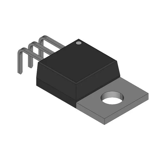
500 V CoolMOS N-channel in a TO-220
These numbers tell a design engineer that the FET can be driven with a modest gate-drive current — 17 nC at 100 kHz switching frequency draws only 1.7 mA from the driver, keeping the gate-drive loss low.
Thermal and operating range
Maximum power dissipation is 66 W at case temperature, with the TO-220 tab providing a direct thermal path to a heatsink — the limiting factor in a real design is the heatsink's thermal resistance, not the die itself.