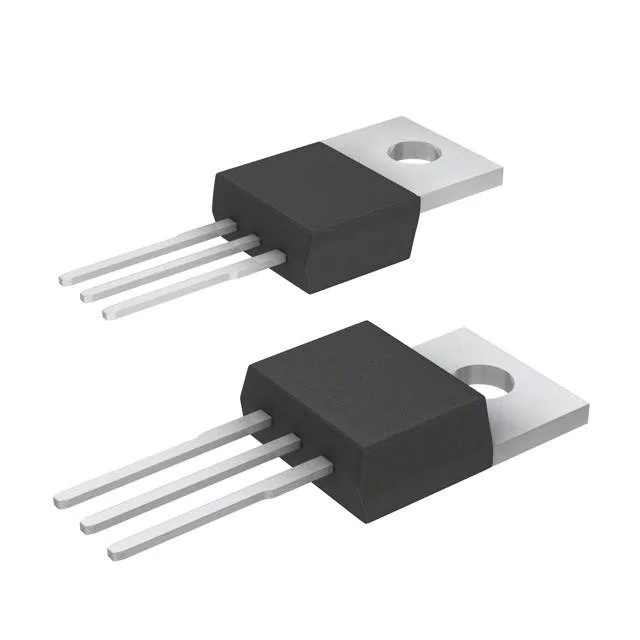
The IPP12CN10LGXKSA1: At 69 A load, the 12 mOhm maximum Rds(on) at Vgs=10 V yields about 57 W conduction loss at the die level before derating for junction temperature. The 5600 pF input capacitance at 50 V Vds is moderate — a typical gate driver with 2 A peak source/sink can turn this device on in the 30–50 ns range.
175°C junction rating — extends the operating envelope
In an automotive under-hood environment or a sealed industrial power supply where ambient air hits 85–105°C, the extra 25°C of junction margin keeps the MOSFET inside its SOA without oversizing the heatsink. The 2.4 V maximum gate threshold at 83 µA drain current means the device is fully enhanced with standard 5 V or 3.3 V logic-level gate drive, though the 12 mOhm Rds(on) is specified at 10 V — a 4.5 V drive will yield a higher on-resistance.