OptiMOS 150 V N-channel — switching and conduction loss budget
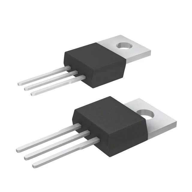
The IPP111N15N3GXKSA1: Housed in the TO-220-3 through-hole package (PG-TO220-3), it suits designs where the PCB is the heatsink interface — the exposed metal tab carries the drain potential and must be electrically isolated or tied to the drain rail. The junction temperature range spans -55 to 175 °C, covering industrial and automotive under-hood environments where the MOSFET sits near the engine block or exhaust manifold.
Gate drive and switching dynamics
Input capacitance Ciss is 3230 pF typical at 75 V drain bias, which together with the 55 nC gate charge determines the switching energy per cycle. A gate resistor in the 10-22 ohm range typically controls the turn-on slew rate without excessive ringing on the TO-220 lead frame. The 150 V Vdss gives headroom above a 48 V or 80 V bus, making this part a candidate for 48 V telecom rectifiers, 72 V battery management systems, and 100 V intermediate bus converters where the steady-state rail sits at 80-90 V and the switching transient stays under 150 V.