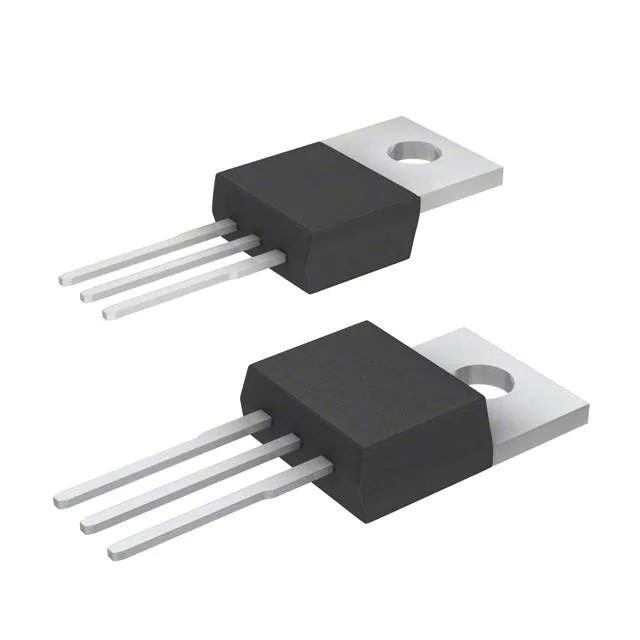
IPP076N15N5AKSA1

Infineon Technologies · OptiMOS™ 5 Series

Infineon OptiMOS™ 5 N-Channel MOSFET, 150 V Vdss, 112 A Id, 7.6 mOhm Rds(on) at 56 A, 10 V, 21 nC Qg, TO-220-3, -55 to 175 °C.

Infineon Technologies IPP076N15N5AKSA1
Download datasheet (PDF)
[IN STOCK] In Stock: 5 pcs
$4.73/ pc

Volume pricing

Buy Now

MOQ 1 · Tube · RoHS · EIA-481 · DAP/DDP · T/T

Technical specifications

IPP076N15N5AKSA1 specifications
Parameter / AttributeSpecification / Value
SeriesOptiMOS™ 5
FET typeN-Channel
MountingThrough Hole
Drain to source voltage150 V
Drive voltage (Max rds on, min rds on)8V, 10V
Current - continuous drain (Id) @ 25°C112A (Tc)
Power dissipation214W (Tc)
Operating temperature-55°C ~ 175°C (TJ)
PackageTube
Vgs±20V
TechnologyMOSFET (Metal Oxide)
FET featureStandard
CaseTO-220-3
Vgs(th) (Max) @ id4.6V @ 160µA
Rds on (Max) @ id, vgs7.6mOhm @ 56A, 10
Gate charge (Qg) (Max) @ vgs21 nC @ 10 V
Input capacitance (Ciss) (Max) @ vds4700 pF @ 75 V

Technical details

7.6 mOhm at 56 A — the conduction-loss anchor

The Infineon IPP076N15N5AKSA1 is an OptiMOS™ 5 N-channel power MOSFET in a through-hole TO-220-3 package.

Total gate charge is 21 nC at Vgs = 10 V. A low Qg for a 112 A-class FET means the gate driver sees a smaller capacitive load per cycle, which translates to faster turn-on and turn-off edges and reduced switching losses in a hard-switched topology like a synchronous buck or a half-bridge. Input capacitance Ciss is 4700 pF at Vds = 75 V. That figure, combined with the 21 nC Qg, gives the designer a handle on the driver peak current needed to hit the target dv/dt without excessive Miller plateau dwell.

Maximum power dissipation is 214 W at case temperature Tc — a number that assumes an ideal heatsink; real designs derate from that ceiling based on the thermal resistance of the chosen heatsink and airflow.

IPP076N15N5AKSA1
[ALLOC] verified
Quote