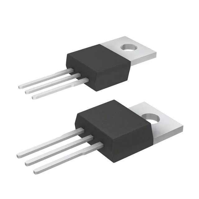
Infineon Technologies IPP040N06NAKSA1

Infineon IPP040N06NAKSA1 OptiMOS N-Channel 60V 80A MOSFET

MPNIPP040N06NAKSA1
End of Life

Infineon OptiMOS N-Channel MOSFET, 60V Vdss, 80A Id at Tc, 4mOhm Rds(on) at 10V, 38nC Qg, -55 to 175°C, TO-220-3 package.

$2.0Ref. price · indicative, final on quote
PackagingTO-220-3
RoHSROHS3 Compliant
SeriesOptiMOS™
Independent supplier — new & surplus stockAuthenticity-screened · ESD-safe packingListing updated Jul 2026

Specifications

IPP040N06NAKSA1 specifications
ParameterValue
SeriesOptiMOS™
FET typeN-Channel
MountingThrough Hole
Drain to source voltage60 V
Drive voltage (Max rds on, min rds on)6V, 10V
Current - continuous drain (Id) @ 25°C20A (Ta), 80A (Tc)
Power dissipation3W (Ta), 107W (Tc)
Operating temperature-55°C ~ 175°C (TJ)
PackageTube
Vgs±20V
TechnologyMOSFET (Metal Oxide)
CaseTO-220-3
Vgs(th) (Max) @ id2.8V @ 50µA
Rds on (Max) @ id, vgs4mOhm @ 80A, 10V
Gate charge (Qg) (Max) @ vgs38 nC @ 10 V
Input capacitance (Ciss) (Max) @ vds2700 pF @ 30 V

Product details

60 V N-channel in a TO-220 — the OptiMOS power switch for 48 V bus rails

The Infineon IPP040N06NAKSA1 is a 60 V N-channel MOSFET from the OptiMOS series, rated for 80 A continuous drain current at the case and 20 A at ambient. The TO-220-3 through-hole package (PG-TO220-3 supplier code) has a metal tab that is electrically the drain terminal. That means the heatsink must either be electrically isolated from the chassis or share the drain potential — a common consideration when bolting the tab to a grounded enclosure.

On-resistance, gate charge, and the drive voltage window

The Rds(on) of 4 mOhm is specified at Id = 80 A and Vgs = 10 V, with the drive voltage range spanning 6 V to 10 V for achieving the minimum on-resistance. A gate driver that cannot swing to 10 V leaves part of the Rds(on) improvement on the table — the 6 V minimum is the floor for the device to turn on hard, but the 10 V level is where the datasheet guarantees the 4 mOhm figure. Total gate charge is 38 nC at a 10 V gate drive. Input capacitance Ciss is 2700 pF measured at Vds = 30 V, which together with the gate charge gives the designer the numbers for calculating the driver's switching loss and the gate-resistor value for slew-rate control.

Junction temperature and thermal design

Bolting it to a heatsink with thermal compound is standard practice; the tab-to-heatsink thermal resistance determines how much of the 107 W case dissipation can actually be pulled out of the device.

Active lifecycle and channel posture

Frequently asked questions

Can the IPP040N06NAKSA1 replace the IRFZ44N?

The IRFZ44N is a 55 V / 49 A N-channel MOSFET in a TO-220 package with a typical Rds(on) around 17.5 mOhm. The IPP040N06NAKSA1 has a higher drain rating (60 V / 80 A) and significantly lower on-resistance (4 mOhm). While both are N-channel TO-220 parts, the gate-drive voltage and switching characteristics differ — verify the gate-driver output swing and the switching speed requirements in your circuit before substituting.