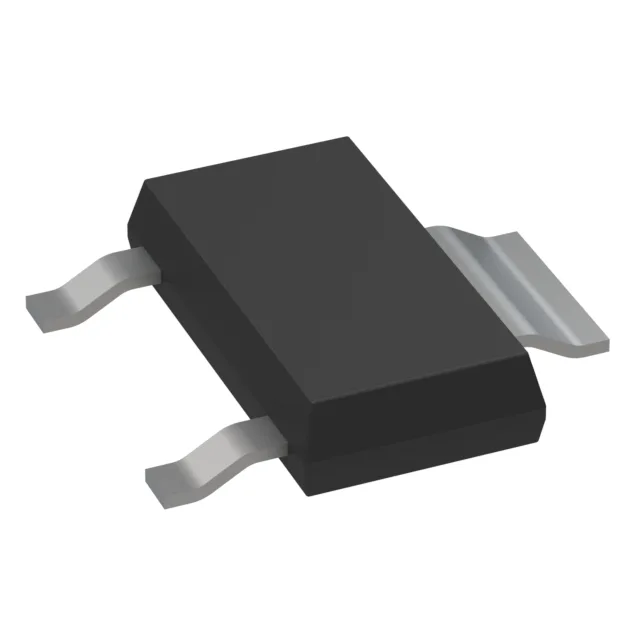
500 V switching in a SOT-223 — what it buys the BOM
The PG-SOT223-3 package is a surface-mount footprint that fits standard reflow profiles, but the 5 W dissipation ceiling means the real-world continuous current is derated significantly above 25°C. For a 500 V device in this small outline, the die-to-ambient thermal path is the binding constraint — not the silicon rating.
Gate drive and switching — the 6 nC advantage
With a typical gate charge of 6 nC at 10 V, this MOSFET presents a light load to the gate driver. A small-signal PWM controller output can drive it directly without a dedicated driver stage, which simplifies the BOM for low-power flyback converters and auxiliary supplies. The input capacitance is 124 pF at 100 V drain-source, keeping the switching node capacitance low for clean waveform edges. The gate threshold voltage is specified at 3.5 V maximum with 50 µA drain current, so a 5 V logic-level gate drive will turn the device on, but the 13 V drive voltage is needed to achieve the rated 2 Ohm Rds(on).
The PG-SOT223-3 package has a standard pinout: gate on pin 1, source on pins 2 and 4 (internally common), drain on pin 3.
The part is ROHS3 compliant. Sourced through independent distribution.