600 V, 33 A, 105 mOhm — the CoolMOS™ P7 sweet spot
Rds(on) is specified at Vgs = 10 V, which is the recommended drive voltage for the CoolMOS series. Driving at 10 V ensures the channel is fully enhanced; at lower gate voltages the on-resistance climbs steeply, and the ±20 V absolute maximum gate rating gives headroom for ringing on the gate node in a hard-switching topology. Input capacitance Ciss is 1952 pF typical at Vds = 400 V. This is a moderate value for a 600 V, 33 A part — it keeps the switching-node dv/dt manageable and reduces the Miller plateau duration. The gate threshold voltage is specified at a maximum of 4 V at Id = 530 µA. This means the device is fully off at Vgs = 0 V (enhancement mode) and begins conducting around 3–4 V. For designs using a 5 V gate drive rail, ensure the driver output reaches at least 8–10 V to minimise Rds(on) — the 4 V Vgs(th) is a turn-on threshold, not an on-state drive level.
RoHS3 compliance is confirmed — no exemptions for lead in solder or other restricted substances, which simplifies compliance declarations for EU and California markets. The CoolMOS series is Infineon's mainstream high-voltage MOSFET platform; the active status and broad installed base mean the part is widely stocked across the independent and authorised distribution network.
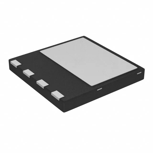
PG-VSON-4 — package and layout considerations
The 4-lead PowerTSFN package (PG-VSON-4) is a surface-mount, leadless package with a large exposed drain pad on the bottom. For a 33 A continuous current, the PCB copper pour on the drain node needs to be sized for the current density and heat spreading, not just the package footprint. The surface-mount mounting type means the part is reflow-soldered. The PG-VSON-4 package is compatible with standard lead-free reflow profiles. No through-hole or press-fit option exists.