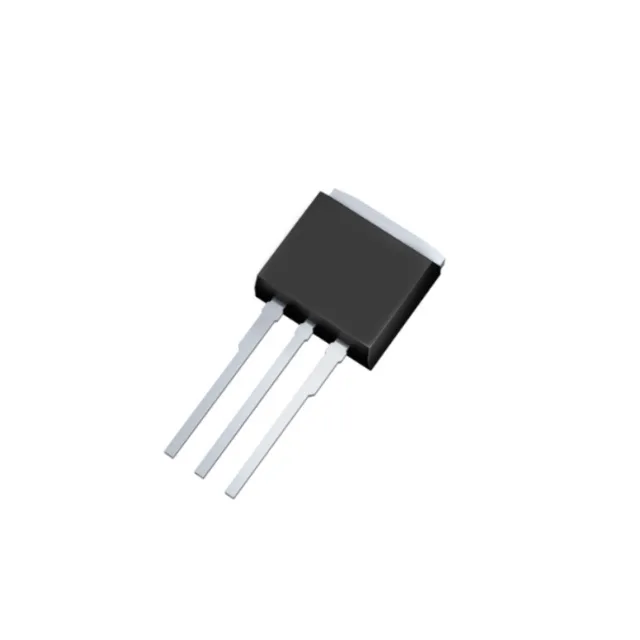
900 V CoolMOS in a through-hole package
It comes in a PG-TO262-3-1 through-hole package — the long-lead I²Pak variant that suits board-level mounting where the tab is soldered to the PCB copper plane for heat sinking. The 340 mOhm maximum on-resistance at 9.2 A with 10 V gate drive is the number to size the conduction losses in a 900 V-class offline converter or PFC stage. At 15 A the Rds(on) will be higher — the datasheet's normalised curve shows the typical increase with current and junction temperature.
Gate charge and switching speed
Total gate charge is 94 nC at 10 V gate drive. For a hard-switched 100 kHz application, the average gate-drive current is about 9.4 mA — well within the capability of a standard driver IC. The 2400 pF input capacitance at 100 V drain-source gives a rough Ciss figure for estimating the driver's peak current requirement during the Miller plateau.
Temperature range and thermal budget
Maximum power dissipation is 208 W at case temperature 25 °C — derate linearly above that. The TO-262 tab is the primary thermal path; the copper area on the PCB under the tab sets the effective RthJA for the real assembly.
