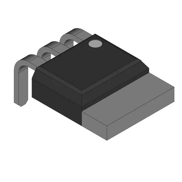
Infineon Technologies IPI126N10N3GXKSA1

IPI126N10N3GXKSA1 N-Channel Power MOSFET, 100 V, 12.6 mOhm

MPNIPI126N10N3GXKSA1
End of Life

Infineon OptiMOS™ 3 IPI126N10N3GXKSA1, N-channel power MOSFET, 100 V Vds, 58 A Id, 12.6 mOhm Rds(on) at 10 V, 35 nC Qg, TO-262-3 through-hole, -55 to 175°C.

$0.64Ref. price · indicative, final on quote
PackagingTO-262-3 Long Leads, I²Pak, TO-262AA
StockContact for availability
MOQ1 pcs
  • 100% new & originalTraceable channels only — no refurbs, no pulls, no remarked parts.
  • Date & lot codes on quoteStated per line before you commit; label photos on request.
  • MSL-compliant ESD packingMoisture-sealed bags with indicator cards; reels photo-verified.
  • PayPal buyer protectionPay by T/T, PayPal or Payoneer — card payments covered end to end.

Specifications

IPI126N10N3GXKSA1 Technical Specifications
ParameterValue
SeriesOptiMOS™ 3
FET typeN-Channel
Mounting typeThrough Hole
Drain to source voltage100 V
Drive voltage (Max rds on, min rds on)6V, 10V
Current - continuous drain (Id) @ 25°C58A (Tc)
Power dissipation94W (Tc)
Operating temperature-55°C ~ 175°C (TJ)
PackageBulk
Vgs±20V
TechnologyMOSFET (Metal Oxide)
CaseTO-262-3 Long Leads, I²Pak, TO-262AA
Vgs(th) (Max) @ id3.5V @ 46µA
Rds on (Max) @ id, vgs12.6mOhm @ 46A, 10V
Gate charge (Qg) (Max) @ vgs35 nC @ 10 V
Input capacitance (Ciss) (Max) @ vds2500 pF @ 50 V

Product details

The 12.6 mOhm maximum on-resistance at 10 V Vgs sets the conduction loss floor for the power stage — at 46 A the dissipation stays under 27 W before factoring in the temperature derating.

Gate charge and switching — 35 nC at 10 V

Total gate charge is 35 nC at 10 V. For a 100 kHz hard-switched converter, the gate drive current needed is roughly 3.5 mA average — well within a standard totem-pole driver — but the peak current from the driver must clear the Miller plateau without slowing the switching edge. Input capacitance Ciss is 2500 pF at 50 V drain bias.

Through-hole TO-262 — mounting and thermal path

The PG-TO262-3 (I²Pak, TO-262AA) package is a through-hole form with long leads. The exposed metal tab on the back provides the primary thermal path to the heatsink or PCB copper — the 94 W power dissipation limit assumes the tab is held at case temperature. Mounting requires a hole or clip for the tab; the three through-hole leads handle the current. For a rework bench, the lead length and tab geometry are standard across the TO-262 family — the footprint matches the common I²Pak land pattern.

Temperature grade and operating envelope

That 175°C ceiling is typical for automotive-grade power MOSFETs — the part can survive under-hood soak temperatures and high-load transients, but the Rds(on) doubles roughly above 100°C junction, so the thermal design must budget for the hot resistance. The gate threshold voltage maximum is 3.5 V at 46 µA drain current. With the recommended drive voltage window of 6 V to 10 V for rated Rds(on), a standard 12 V gate drive from a PWM controller or gate driver IC fully enhances the channel.

Lifecycle and sourcing posture

Infineon continues to manufacture the OptiMOS 3 series in this voltage class.

Frequently asked questions

What is the exact Rds(on) of IPI126N10N3GXKSA1 at 10 V Vgs?

The maximum on-resistance at 10 V Vgs and 46 A drain current is 12.6 mOhm. This is the worst-case value at 25°C junction temperature — the typical value is lower, but the BOM should budget for the 12.6 mOhm ceiling.

Does IPI126N10N3GXKSA1 have a direct replacement or equivalent?

No official second-source or direct replacement is listed on the record for this specific order code. The peer IPD50R950CEAUMA1 is a 500 V CoolMOS CE device in a surface-mount package — different voltage class and mounting, so not a functional substitute.