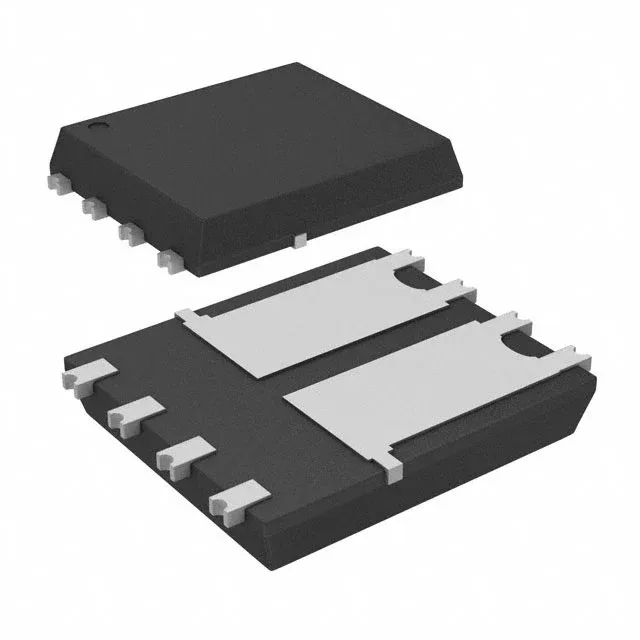
Infineon Technologies IPG20N06S2L65AATMA1

IPG20N06S2L65AATMA1 Infineon OptiMOS™ Dual N-Channel MOSFET

MPNIPG20N06S2L65AATMA1
End of Life

Infineon OptiMOS™ IPG20N06S2L65AATMA1, dual N-channel automotive MOSFET, 55V Vdss, 20A Id, 65mOhm Rds(on) at 15A, logic-level gate, PG-TDSON-8-10 wettable flank package, -55°C to 175°C.

$1.1Ref. price · indicative, final on quote
Packaging8-PowerVDFN
StockContact for availability
MOQ1 pcs
  • 100% new & originalTraceable channels only — no refurbs, no pulls, no remarked parts.
  • Date & lot codes on quoteStated per line before you commit; label photos on request.
  • MSL-compliant ESD packingMoisture-sealed bags with indicator cards; reels photo-verified.
  • PayPal buyer protectionPay by T/T, PayPal or Payoneer — card payments covered end to end.

Specifications

IPG20N06S2L65AATMA1 Technical Specifications
ParameterValue
SeriesOptiMOS™
Mounting typeSurface Mount, Wettable Flank
Drain to source voltage55V
Current - continuous drain (Id) @ 25°C20A
Power - max43W
Operating temperature-55°C ~ 175°C (TJ)
GradeAutomotive
PackageTape & Reel (TR); Cut Tape (CT)
TechnologyMOSFET (Metal Oxide)
FET featureLogic Level Gate
Configuration2 N-Channel (Dual)
QualificationAEC-Q101
Case8-PowerVDFN
Vgs(th) (Max) @ id2V @ 14µA
Rds on (Max) @ id, vgs65mOhm @ 15A, 10V
Gate charge (Qg) (Max) @ vgs12nC @ 10V
Input capacitance (Ciss) (Max) @ vds410pF @ 25V

Product details

Dual 55V N-channel in a single TDSON-8 — the BOM-fit tier

The Infineon IPG20N06S2L65AATMA1 is a dual N-channel automotive MOSFET from the OptiMOS™ series, integrating two 55V-rated switches in one PG-TDSON-8-10 package with wettable flanks for solder-joint inspection.

65mOhm Rds(on) — where it lands in the OptiMOS 55V dual family

This is the mid-Rds(on) option in Infineon's 55V dual N-channel line. The 65mOhm per-channel figure sits between the 50mOhm IPG20N06S2L50AATMA1 and the 35mOhm IPG20N06S2L35AATMA1, all in the same PG-TDSON-8-10 footprint. The trade-off is conduction loss versus gate charge: the 65mOhm part draws 12nC total gate charge at 10V, while the 35mOhm sibling needs 23nC — a meaningful difference for a microcontroller GPIO driving the gate directly without a pre-driver.

Wettable-flank TDSON-8 — AOI-friendly power package

The PG-TDSON-8-10 is a 8-pin power DFN with an exposed die pad on the bottom. The wettable-flank feature means the side edges of the package terminals are plated so that solder fillets form visible menisci — automated optical inspection (AOI) can verify the solder joint quality, which is a requirement in many automotive production lines where bottom-only terminations are otherwise hidden. The 43W maximum power dissipation assumes the PCB copper area under the pad is sized for thermal spreading; the datasheet's RthJA curve is the reference for the actual board stack-up.

Frequently asked questions

Is IPG20N06S2L65AATMA1 compatible with 3.3V logic?

Yes. The logic-level gate feature gives a maximum gate threshold voltage of 2V at 14µA, so a 3.3V microcontroller output can fully enhance the channel. The 10V gate-drive condition for the 65mOhm Rds(on) spec is the optimal bias for lowest on-resistance, but the part will switch at 3.3V with a higher Rds(on) — check the transfer characteristic curve in the datasheet for the exact value at your gate voltage.

What is the cross reference for IPG20N06S2L65AATMA1?

The IPG20N06S2L65ATMA1 is a functional cross-reference — same 55V/20A/65mOhm ratings, same AEC-Q101 grade, same OptiMOS™ series. The difference is the package: the AATMA1 suffix has wettable flanks for AOI; the ATMA1 suffix uses a standard TDSON-8 without wettable flanks. Check your assembly line's solder-joint inspection requirements before substituting.