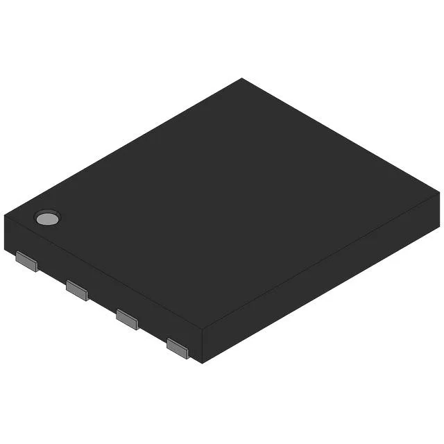
Infineon Technologies IPG20N04S412AATMA1

IPG20N04S412AATMA1 OptiMOS™ Dual N-Channel MOSFET, 40V 20A

MPNIPG20N04S412AATMA1
End of Life

Infineon OptiMOS™ IPG20N04S412AATMA1, dual N-channel MOSFET, 40V Vdss, 20A continuous drain, 12.2mOhm Rds(on) @ 17A, 10V, PG-TDSON-8-10, AEC-Q101, -55°C to 175°C.

$1.26Ref. price · indicative, final on quote
Packaging8-PowerVDFN
StockContact for availability
MOQ1 pcs
  • 100% new & originalTraceable channels only — no refurbs, no pulls, no remarked parts.
  • Date & lot codes on quoteStated per line before you commit; label photos on request.
  • MSL-compliant ESD packingMoisture-sealed bags with indicator cards; reels photo-verified.
  • PayPal buyer protectionPay by T/T, PayPal or Payoneer — card payments covered end to end.

Specifications

IPG20N04S412AATMA1 Technical Specifications
ParameterValue
SeriesOptiMOS™
Mounting typeSurface Mount, Wettable Flank
Drain to source voltage40V
Current - continuous drain (Id) @ 25°C20A
Power - max41W
Operating temperature-55°C ~ 175°C (TJ)
GradeAutomotive
PackageTape & Reel (TR); Cut Tape (CT)
TechnologyMOSFET (Metal Oxide)
Configuration2 N-Channel (Dual)
QualificationAEC-Q101
Case8-PowerVDFN
Vgs(th) (Max) @ id4V @ 15µA
Rds on (Max) @ id, vgs12.2mOhm @ 17A, 10V
Gate charge (Qg) (Max) @ vgs18nC @ 10V
Input capacitance (Ciss) (Max) @ vds1470pF @ 25V

Product details

12.2 mOhm Rds(on) — the conduction-loss floor for a 40 V dual switch

The Infineon IPG20N04S412AATMA1 is a dual N-channel MOSFET from the OptiMOS™ family, rated 40 V drain-to-source and 20 A continuous drain at 25°C. Its on-resistance is specified at 12.2 mOhm maximum with a 17 A drain current and 10 V gate drive — that is the conduction-loss floor for a 40 V dual switch in a PG-TDSON-8-10 package. AEC-Q101 qualification and a 175°C junction temperature rating place it in automotive under-hood and chassis-domain applications where both reliability and thermal headroom are non-negotiable.

The PG-TDSON-8-10 package includes a wettable flank, which means the side pads accept solder and are visible to automated optical inspection after reflow. For automotive production lines that require AOI coverage on every joint, this eliminates the need for X-ray inspection on hidden solder fillets.

Gate charge and input capacitance — the driver budget

Maximum gate charge is 18 nC at 10 V, and input capacitance is 1470 pF at 25 V drain-to-source. A 100 kHz switching frequency with 18 nC gate charge draws 1.8 mA from the gate driver per channel — well within the capability of a standard automotive gate-driver IC. The 1470 pF Ciss means the driver sees a moderate capacitive load; no special high-current driver is needed for the target switching speed.

Frequently asked questions

What is the Rds(on) of IPG20N04S412AATMA1?

The maximum on-resistance is 12.2 mOhm at a drain current of 17 A and a gate-to-source voltage of 10 V. This is the conduction-loss floor for the dual switch at the specified bias point.

Is IPG20N04S412AATMA1 AEC-Q101 qualified?

Yes, the part is AEC-Q101 qualified, which means it meets the automotive stress and reliability requirements for under-hood and chassis-domain applications.

Does IPG20N04S412AATMA1 have a wettable flank?

Yes, the PG-TDSON-8-10 package includes a wettable flank, enabling automated optical inspection of solder joints after reflow.