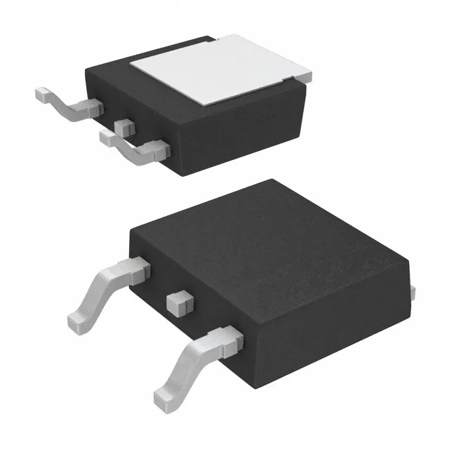
30 V automotive-grade N-channel MOSFET in DPAK
Built on a metal-oxide semiconductor process and qualified to AEC-Q101, it is designed for automotive load switching, DC-DC converters, and motor-drive pre-drive stages where junction temperatures can reach 175°C. The on-resistance maxes at 6.4 mOhm with a 10 V gate drive, which keeps conduction losses manageable in a 50 A path — a key figure when sizing heatsinks or PCB copper for a 136 W dissipation budget. Gate charge is 68 nC at 10 V, so the driver stage should be sized to deliver that charge within the switching period without excessive cross-conduction. The part comes in a PG-TO252-3-11 (DPAK) surface-mount package with a tab for thermal transfer to the board. The 4.5 V minimum drive voltage allows logic-level gate signals, though the full Rds(on) spec is characterised at 10 V.
Input capacitance of 1900 pF at 25 V drain-source is moderate — it does not demand an aggressive gate driver but does contribute to switching losses at higher frequencies. The 68 nC gate charge at 10 V tells you the total charge the driver must source per cycle; pair it with a driver capable of sourcing that charge in the desired switching time to avoid excessive miller plateau dwell.
The PG-TO252-3-11 footprint is standard for DPAK devices, so board-level re-spin is not needed if a second-source candidate shares the same package and pinout. No official second-source alternate is listed in the Infineon cross-reference for this order code.