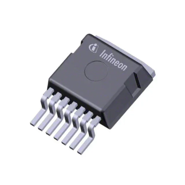
650 V N-channel CoolMOS for automotive high-voltage switching
The IPBE65R230CFD7AATMA1: The 230 mOhm on-resistance at 10 V gate drive keeps conduction losses manageable for a 650 V class part, and the 23 nC typical gate charge at 10 V means the gate driver doesn't need to push much current for fast switching. Input capacitance is 1044 pF at 400 V drain bias — a figure that matters when sizing the gate drive loop for EMI and switching loss trade-offs.
Package and rework — the TO-263-7 reality
This is a TO-263-7 (D²Pak) with six leads and a large exposed drain tab. Rework with hot air is possible if the board has adequate bottom-side preheat; the tab's thermal mass means it'll take longer to reflow than a small-signal SOIC. Lift the part, not the pad — the tab solder joint is the one that'll tear a pad if you rush it.
It is ROHS3 compliant.