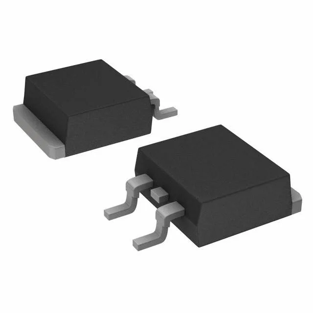
900 V CoolMOS in a D2PAK — what you get
It comes in a TO-263-3 (D2PAK) surface-mount package, which is the same footprint as the industry-standard D2PAK but with Infineon's PG-TO263-3-2 variant.
Switching losses and gate drive
Total gate charge is 94 nC at 10 V gate drive. For a 100 kHz switching frequency, the average gate-drive current needed is about 9.4 mA — well within the capability of a standard MOSFET driver IC. The input capacitance Ciss is 2400 pF at 100 V drain-source, which influences the turn-on delay and the driver's peak current requirement. The ±20 V maximum gate-source rating gives headroom for gate-drive overshoot in hard-switching topologies.
Thermal budget and package handling
Maximum power dissipation is 208 W at case temperature, but the real limit is set by the junction-to-case thermal resistance and the board's ability to sink heat through the D2PAK tab. The operating junction temperature range is -55 °C to 150 °C, so derating for ambient temperature above 25 °C is required. The D2PAK tab is the main heat path — a copper pour on the PCB under the tab, with vias to an inner-layer or backside copper plane, is the standard layout practice.
Lifecycle and compliance
The series is CoolMOS™, Infineon's high-voltage MOSFET platform with multiple voltage classes; this 900 V variant targets the upper end of the 600 V–900 V range.
Sourcing posture
Sourced through independent distribution channels. No minimum order threshold beyond what the distributor sets for the package form factor — Tape & Reel or Cut Tape.
