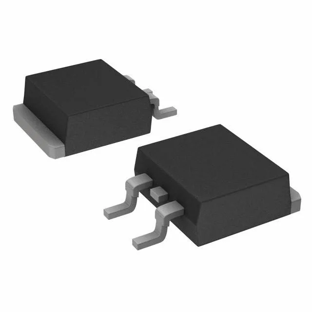
40 V N-channel OptiMOS — what the 2.1 mOhm Rds(on) buys you
Gate charge and switching — what 118 nC means for the driver
With a maximum gate charge of 118 nC at 10 V, the IPB90N04S402ATMA1 requires a gate driver capable of sourcing and sinking that charge within the target switching period — a 118 nC gate at 100 kHz draws about 11.8 mA average from the driver, well within the capability of most dedicated MOSFET drivers. The input capacitance is 9430 pF at 25 V drain-source, which influences the turn-on and turn-off delay times; the driver output impedance and gate resistor should be selected to keep the switching edges clean and avoid Miller plateau ringing.
Reworking a D²Pak on a hot-air station is straightforward if the board has adequate copper soak: preheat the board to 125°C, apply hot air to the tab until the solder reflows, then lift the part with tweezers — the tab's thermal mass means you need a nozzle that covers the full body, not a pencil tip.