10.7 mOhm at 40 A — the conduction-loss anchor
The IPB80N06S2L11ATMA2: The 10.7 mOhm maximum on-resistance at Vgs=10 V and 40 A sets the conduction-loss floor for the design. This part targets high-current switching and OR-ing functions in automotive and industrial power stages where the 175 °C junction rating provides headroom under overload.
Total gate charge Qg is 80 nC at Vgs=10 V. The 2075 pF input capacitance at Vds=25 V sets the Miller plateau charge time; a driver with 2 A peak source/sink keeps the switching edges clean. The drive voltage window spans 4.5 V to 10 V — the 10.7 mOhm rating is specified at 10 V, but the part can be driven from a 5 V logic rail with higher Rds(on).
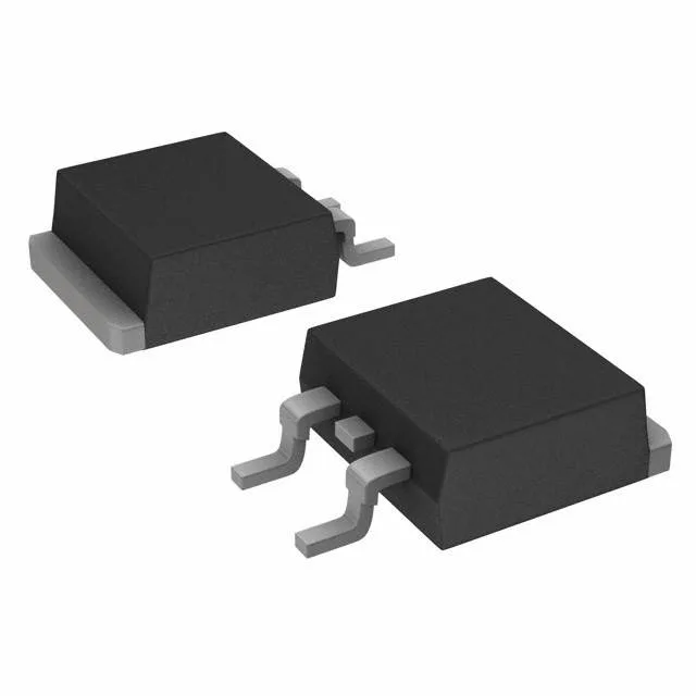
Housed in the PG-TO263-3-2 (D²Pak) surface-mount package, the large copper tab provides the primary thermal path to the PCB. Maximum power dissipation is 158 W at Tc=25 °C.