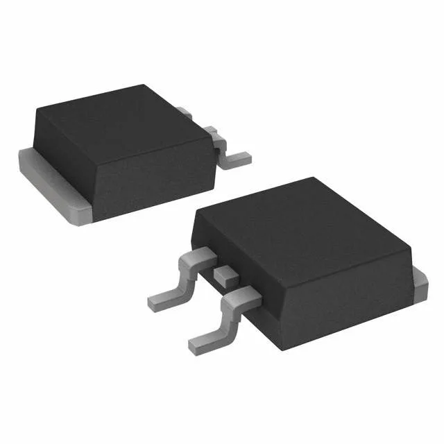
Infineon Technologies IPB70N10S312ATMA1

IPB70N10S312ATMA1 N-Channel MOSFET 100V 70A TO-263-3

MPNIPB70N10S312ATMA1
End of Life

Infineon OptiMOS IPB70N10S312ATMA1, N-Channel MOSFET, 100 V Vdss, 70 A Id, 11.3 mOhm Rds(on) @ 70 A, 10 V, PG-TO263-3-2 package, -55°C to 175°C junction temperature.

$2.9Ref. price · indicative, final on quote
PackagingTO-263-3, D²Pak (2 Leads + Tab), TO-263AB
StockContact for availability
MOQ1 pcs
  • 100% new & originalTraceable channels only — no refurbs, no pulls, no remarked parts.
  • Date & lot codes on quoteStated per line before you commit; label photos on request.
  • MSL-compliant ESD packingMoisture-sealed bags with indicator cards; reels photo-verified.
  • PayPal buyer protectionPay by T/T, PayPal or Payoneer — card payments covered end to end.

Specifications

IPB70N10S312ATMA1 Technical Specifications
ParameterValue
SeriesOptiMOS™
FET typeN-Channel
Mounting typeSurface Mount
Drain to source voltage100 V
Drive voltage (Max rds on, min rds on)10V
Current - continuous drain (Id) @ 25°C70A (Tc)
Power dissipation125W (Tc)
Operating temperature-55°C ~ 175°C (TJ)
PackageTape & Reel (TR); Cut Tape (CT)
Vgs±20V
TechnologyMOSFET (Metal Oxide)
CaseTO-263-3, D²Pak (2 Leads + Tab), TO-263AB
Vgs(th) (Max) @ id4V @ 83µA
Rds on (Max) @ id, vgs11.3mOhm @ 70A, 10V
Gate charge (Qg) (Max) @ vgs66 nC @ 10 V
Input capacitance (Ciss) (Max) @ vds4355 pF @ 25 V

Product details

The 66 nC total gate charge at 10 V is moderate for this current class; a gate driver delivering 1 A can switch it in about 66 ns, making it suitable for hard-switching converters up to the 100 kHz range.

Junction temperature range — where it fits

The 175°C ceiling is 25°C above the typical industrial 150°C limit, giving extra headroom in under-hood automotive, high-ambient industrial enclosures, or power supplies with tight thermal budgets. The 4 V maximum gate threshold at 83 µA drain current means the device is fully enhanced with a standard 10 V gate drive; at lower gate voltages the Rds(on) will be higher than the 11.3 mOhm spec.

Package and footprint — TO-263-3 (D²Pak)

Housed in the PG-TO263-3-2 package — a surface-mount D²Pak with two leads plus the exposed drain tab. The tab is the primary thermal path; the PCB copper area under it sets the junction-to-ambient thermal resistance. The 0.50 mm lead pitch and standard footprint are shared across many 100 V N-channel MOSFETs, so layout reuse across second-source candidates is straightforward.

Frequently asked questions

Is the IPB70N10S312ATMA1 suitable for high-temperature environments?

Yes. The 175°C maximum gives 25°C of margin above the typical industrial 150°C limit.

Is the IPB70N10S312ATMA1 lead-free and RoHS compliant?

Yes, it is ROHS3 compliant, meaning it meets the latest RoHS directive without exemptions for lead, mercury, cadmium, and other restricted substances.

What is the difference between the IPB70N10S312ATMA1 and the IPD50R950CEAUMA1?

The IPD50R950CEAUMA1 is a 500 V CoolMOS device rated at 4.3 A with 950 mOhm Rds(on), while the IPB70N10S312ATMA1 is a 100 V OptiMOS rated at 70 A with 11.3 mOhm. They serve different voltage and current classes — the IPD50R950CEAUMA1 is for high-voltage auxiliary supplies, the IPB70N10S312ATMA1 for low-voltage high-current power stages. They are not direct replacements.