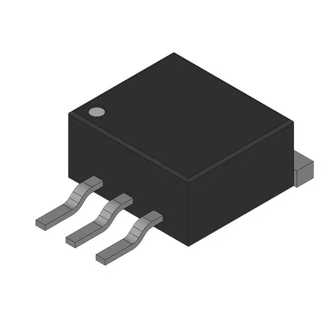
Infineon Technologies IPB65R660CFDAATMA1

Infineon IPB65R660CFDAATMA1 CoolMOS N-Ch MOSFET, 650 V, 6 A

MPNIPB65R660CFDAATMA1
End of Life

Infineon CoolMOS™ IPB65R660CFDAATMA1, N-Channel MOSFET, 650 V Vdss, 6 A Id, 660 mOhm Rds(on) at 10 V, PG-TO263-3 (D2PAK), Automotive Grade, AEC-Q101 Qualified.

$2.51Ref. price · indicative, final on quote
PackagingTO-263-3, D²Pak (2 Leads + Tab), TO-263AB
StockContact for availability
MOQ1 pcs
  • 100% new & originalTraceable channels only — no refurbs, no pulls, no remarked parts.
  • Date & lot codes on quoteStated per line before you commit; label photos on request.
  • MSL-compliant ESD packingMoisture-sealed bags with indicator cards; reels photo-verified.
  • PayPal buyer protectionPay by T/T, PayPal or Payoneer — card payments covered end to end.

Specifications

IPB65R660CFDAATMA1 Technical Specifications
ParameterValue
SeriesCoolMOS™
FET typeN-Channel
Mounting typeSurface Mount
Drain to source voltage650 V
Drive voltage (Max rds on, min rds on)10V
Current - continuous drain (Id) @ 25°C6A (Tc)
Power dissipation62.5W (Tc)
Operating temperature-40°C ~ 150°C (TJ)
GradeAutomotive
PackageTape & Reel (TR); Cut Tape (CT)
Vgs±20V
TechnologyMOSFET (Metal Oxide)
QualificationAEC-Q101
CaseTO-263-3, D²Pak (2 Leads + Tab), TO-263AB
Vgs(th) (Max) @ id4.5V @ 200µA
Rds on (Max) @ id, vgs660mOhm @ 3.2A, 10V
Gate charge (Qg) (Max) @ vgs20 nC @ 10 V
Input capacitance (Ciss) (Max) @ vds543 pF @ 100 V

Product details

It comes in the PG-TO263-3 (D2PAK) surface-mount package and carries AEC-Q101 qualification, making it suitable for automotive-grade power conversion stages — on-board chargers, DC-DC converters, and PFC circuits where the bus voltage sits at 400 V nominal and the ambient under-hood temperature reaches 150 °C junction.

660 mOhm on-resistance — conduction loss at the operating point

At the full 6 A rating, the conduction loss is I²R = 6² × 0.66 ≈ 23.8 W, which sits inside the 62.5 W power dissipation limit at case temperature but leaves a narrow margin for derating at elevated junction temperature — the datasheet's normalised Rds(on) curve will show the multiplier at 150 °C. The gate charge is 20 nC total at 10 V, and the input capacitance is 543 pF at 100 V drain-source. These numbers mean a standard gate driver with 1 A peak output can switch this part at 100 kHz with a few ns of rise time — no need for a high-current booster stage.

AEC-Q101 and the automotive bill of materials

For a BOM that needs a 650 V MOSFET in a D2PAK for an automotive ECU or a traction inverter auxiliary supply, the AEC-Q101 stamp is the gatekeeper for PPAP submission. The part is ROHS3 compliant.

Package and footprint — D2PAK rework considerations

The PG-TO263-3 (D2PAK) is a surface-mount package with two leads plus the tab. For rework, the large tab requires a preheat zone around 150 °C and a hot-air nozzle that covers the full body; a standard soldering iron on the leads alone will not reflow the tab joint.

Frequently asked questions

What is the closest functional alternative to IPB65R660CFDAATMA1?

The IPD50R950CEAUMA1 is a CoolMOS CE N-channel MOSFET in a DPAK package, rated at 500 V drain-source and 4.3 A continuous drain current, with 950 mOhm Rds(on). It is not a pin-compatible second source — the package and voltage rating differ. For a drop-in replacement at 650 V, look at other CoolMOS CFD2 or P7 series parts in D2PAK with similar Rds(on) and gate charge.