In a 2 A offline flyback primary switch, that resistance contributes roughly 1.7 W of I²R loss at full load — within the 83.3 W package power dissipation ceiling, but the designer must account for the Rds(on) positive temperature coefficient when the junction climbs above 25°C.
Total gate charge is 31.5 nC at 10 V, with an input capacitance of 870 pF measured at 100 V drain-source. The low Qg relative to the 650 V class keeps crossover switching losses manageable, which matters for PFC stages and LLC converters where the MOSFET sees both hard turn-on and zero-voltage transitions.
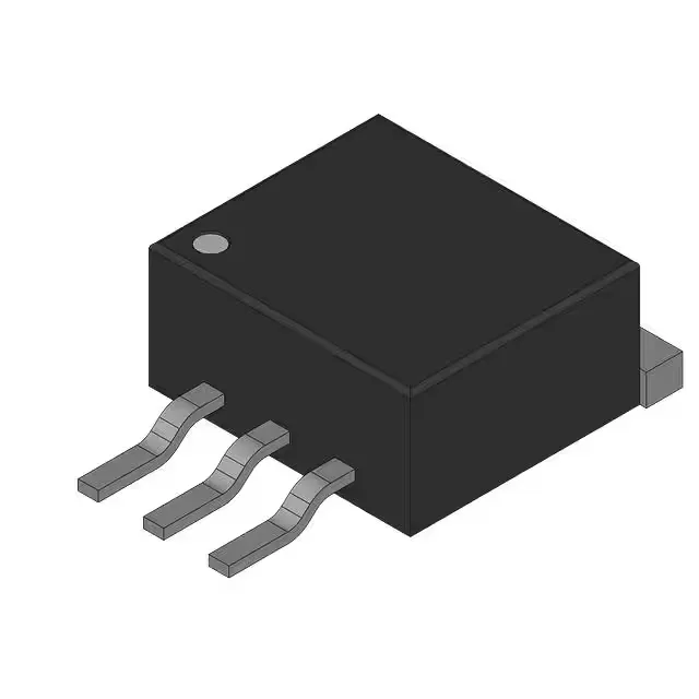
The part ships in a TO-263-3 (D²Pak) surface-mount package, supplier device code PG-TO263-3-2.
It is ROHS3 compliant.