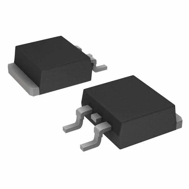
Infineon Technologies IPB65R230CFD7AATMA1 — Analog & Data Acquisition

Infineon IPB65R230CFD7AATMA1 CoolMOS N-Ch MOSFET, 650V

MPNIPB65R230CFD7AATMA1
End of Life

Infineon CoolMOS™ IPB65R230CFD7AATMA1, N-Channel MOSFET, 650 V Vdss, 230 mOhm Rds(on) at 10 V, 11 A continuous drain, PG-TO263-3 package, -40 to 150 °C junction temperature.

$3.28Ref. price · indicative, final on quote
PackagingPG-TO263-3
StockContact for availability
MOQ1 pcs
  • 100% new & originalTraceable channels only — no refurbs, no pulls, no remarked parts.
  • Date & lot codes on quoteStated per line before you commit; label photos on request.
  • MSL-compliant ESD packingMoisture-sealed bags with indicator cards; reels photo-verified.
  • PayPal buyer protectionPay by T/T, PayPal or Payoneer — card payments covered end to end.

Specifications

IPB65R230CFD7AATMA1 Technical Specifications
ParameterValue
SeriesCoolMOS™
FET typeN-Channel
Mounting typeSurface Mount
Drain to source voltage650 V
Drive voltage (Max rds on, min rds on)10V
Current - continuous drain (Id) @ 25°C11A (Tc)
Power dissipation63W (Tc)
Operating temperature-40°C ~ 150°C (TJ)
PackageTape & Reel (TR); Cut Tape (CT)
Vgs±20V
TechnologyMOSFET (Metal Oxide)
Vgs(th) (Max) @ id4.5V @ 260µA
Rds on (Max) @ id, vgs230mOhm @ 5.2A, 10V
Gate charge (Qg) (Max) @ vgs23 nC @ 10 V
Input capacitance (Ciss) (Max) @ vds1044 pF @ 400 V

Product details

Gate drive and switching — what the numbers mean for the design

Gate charge is 23 nC at 10 V, which keeps gate-drive losses manageable in hard-switched topologies like PFC boost stages or LLC resonant converters. Input capacitance is 1044 pF at 400 V drain bias — a figure that directly influences the switching energy and the required gate-drive source/sink capability. The ±20 V maximum gate-to-source rating provides margin against ringing on the gate node; nominal is not absolute max, so keep the gate drive within the ±20 V limit even during transients.

Automotive qualification and thermal limits

The description flags this as an automotive-grade CoolMOS device, which implies AEC-Q101 qualification and the 150 °C maximum junction temperature needed for engine-bay or transmission-mounted inverters. Power dissipation is rated at 63 W at case temperature — that figure assumes an infinite heatsink; real-world derating follows the thermal resistance from junction to case, which the datasheet provides. The 4.5 V maximum gate threshold at 260 µA drain current is a cold-start consideration: at low temperature the threshold rises, so the gate-drive supply must still guarantee 10 V at the gate even with a cold MOSFET.

Package and mounting — PG-TO263-3

The PG-TO263-3 (D²PAK) is a surface-mount package with a large exposed drain tab for thermal transfer to the PCB copper plane. For the 63 W dissipation capability, the PCB layout must provide a low-thermal-resistance path — typically a multi-layer board with thermal vias under the tab. The part is supplied in Tape & Reel or Cut Tape options, which suits both prototyping and automated assembly lines.

Frequently asked questions

What is the Rds(on) of IPB65R230CFD7AATMA1 at 10 V?

The maximum Rds(on) is 230 mOhm at 10 V gate drive with 5.2 A drain current. This is the rated on-resistance for the nominal 10 V drive condition.

Can IPB65R230CFD7AATMA1 be used in automotive applications?

Yes, the device is explicitly designated as automotive-grade CoolMOS, which implies AEC-Q101 qualification. The -40 °C to 150 °C junction temperature range supports under-hood environments.

Is IPB65R230CFD7AATMA1 RoHS compliant?

Yes, it is ROHS3 Compliant.

What is the replacement or equivalent for IPB65R230CFD7AATMA1?

There is no direct replacement listed. The CoolMOS CE family includes the IPD50R950CEAUMA1 (500 V, 950 mOhm), but that is a lower-voltage, higher-resistance device and not a pin-compatible substitute. For a same-spec replacement, look for another CoolMOS CFD7 part with 650 V, 230 mOhm, and PG-TO263-3 package.