With a total gate charge of 93 nC at 10 V, the gate-drive power requirement stays moderate — a driver delivering 1 A peak can switch this FET in the 50–100 kHz range without excessive cross-conduction.
Input capacitance Ciss is 4340 pF at 400 V drain bias. This is a typical figure for a 650 V FET in this Rds(on) bracket; the driver must supply the gate charge during the Miller region, not just the Ciss charging current.
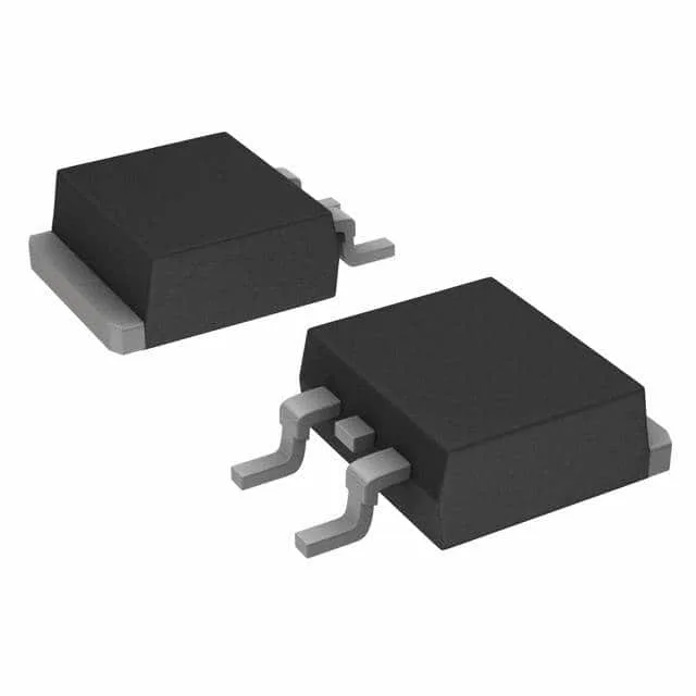
Package and thermal path — TO-263-3 (D²Pak)
The part comes in a TO-263-3 (D²Pak) surface-mount package, supplier device code PG-TO263-3.