Total gate charge is 31 nC at 10 V, which is moderate for a 6.8 A FET — a typical gate driver with 1 A peak source/sink can switch this device in under 100 ns, keeping crossover losses manageable in a 100 kHz hard-switched converter. Input capacitance Ciss is 630 pF at 100 V drain bias, so the gate drive loop sees a light capacitive load that simplifies layout.
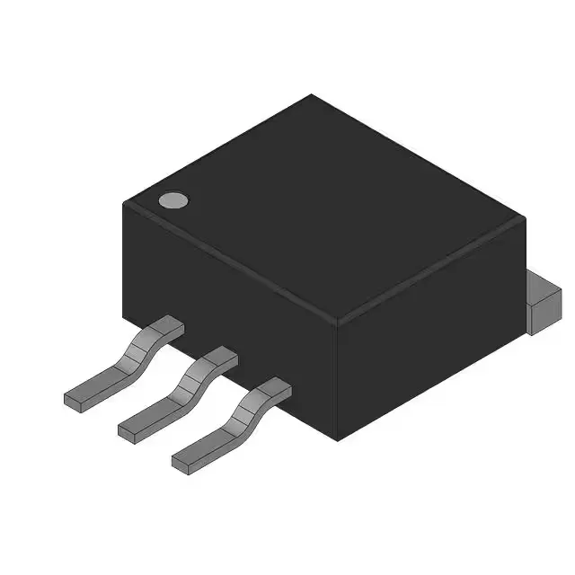
Housed in the PG-TO263-3-2 (D²Pak) surface-mount package, the IPB60R520CP dissipates up to 66 W at case temperature. The large copper tab on the D²Pak couples to the PCB copper plane — a 1 oz pour of at least 25 mm² under the tab keeps the junction below 125°C at 6.8 A continuous.