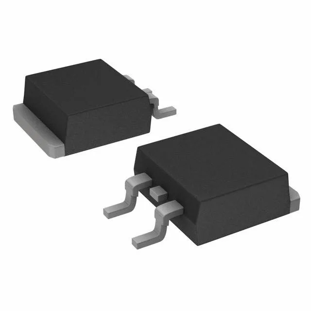
600 V, 13.8 A, 280 mOhm — the PFC and flyback sweet spot
The 280 mOhm maximum on-resistance at 5.2 A, 10 V gate drive places it in the mid-Rds(on) band of the 600 V CoolMOS family — a natural fit for continuous-conduction-mode PFC boost stages, flyback primary switches in adapters, and LLC half-bridge topologies where the conduction loss and switching loss need balancing.
Gate charge and capacitance — light load on the driver
With a typical gate charge of 25.5 nC at 10 V and input capacitance of 1190 pF at 100 V drain bias, this MOSFET presents a light reactive load to the gate driver. A 1 A gate driver IC can charge the gate to the 10 V plateau in roughly 25 ns, keeping cross-conduction intervals short in hard-switched topologies. The low Qg also reduces the gate-drive power loss at high switching frequencies — a practical advantage when pushing a 100 kHz PFC stage.
D²Pak rework — will it survive the hot air?
The PG-TO263-3 (D²Pak) package has a large exposed copper tab that sinks heat into the board. For rework, preheat the board to 125–150°C before hitting the tab with hot air; the tab's thermal mass will pull heat away from the solder joints if you go in cold. The three leads are wide enough that a chisel tip on a soldering iron can wet them individually, but the tab reflow is what makes or breaks the repair. A good thermal via array under the tab is your friend — without it the tab floats and the joint cracks on cool-down.