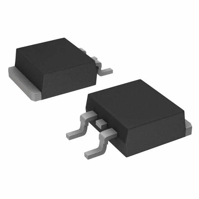
100 V, 35 A N-channel in D2PAK — automotive-grade switching
The Infineon IPB35N10S3L26ATMA1 is an N-channel enhancement-mode MOSFET from the OptiMOS™ family, built on a trench-FET process that balances low on-resistance with fast switching.
On-resistance and gate charge — switching loss trade-off
The 26.3 mOhm Rds(on) at 10 V gate drive is the key conduction loss spec; at 35 A the dissipation is I²R = 32.2 W, which needs to be managed against the 71 W power dissipation limit at the case. The gate charge (Qg) is 39 nC at 10 V — a moderate value that keeps the gate-drive power reasonable for switching frequencies up to several tens of kHz without requiring a high-current driver.
It is ROHS3 compliant.