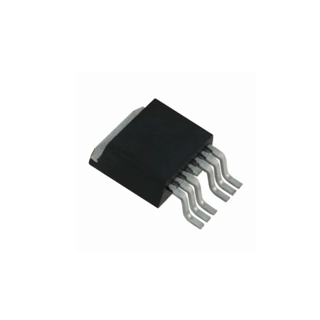
40 V, 180 A N-channel — the load-switch floor
The 1.3 mOhm max on-resistance at 100 A, 10 V drive is the headline number — it sets the conduction-loss floor for a high-current load switch or OR-ing application. The TO-263-7 (D²Pak) package with six leads plus a tab gives the thermal path to the board; the exposed pad is the primary heat-removal route.
Gate charge and switching — what 176 nC means for the driver
Total gate charge is 176 nC at 10 V. The input capacitance of 14000 pF at 25 V Vds reinforces the need for a driver stage between the PWM controller and the gate.
Thermal budget — 188 W dissipation ceiling
In a real board, the junction-to-ambient thermal resistance depends on the copper area under the D²Pak tab and any forced airflow.
ROHS3 compliant.