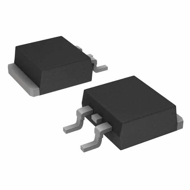
120 V, 56 A N-channel — the OptiMOS power switch
The Infineon IPB144N12N3GATMA1 is an N-channel enhancement-mode power MOSFET from the OptiMOS series, built on a standard metal-oxide semiconductor process. At full rated current the I²R loss is about 45 W, which the 107 W package power dissipation can handle with adequate heatsinking, but the junction temperature rise must be checked against the 175 °C absolute maximum.
Gate drive and switching — 49 nC total gate charge
Total gate charge of 49 nC at 10 V is moderate for a 120 V, 56 A part. A gate driver sourcing 1 A can charge the gate in about 49 ns, but the 3220 pF input capacitance at 60 V drain means the driver sees a capacitive load that rises with the Miller plateau. Practical switching frequencies in hard-switched topologies will land in the 50–150 kHz range before gate-drive losses dominate the thermal budget. The 4 V gate-threshold maximum at 61 µA drain current is a typical logic-level threshold — the part is not a sub-2.5 V logic-level device. The datasheet drive voltage for rated Rds(on) is 10 V, so a 12 V gate-drive rail is the natural choice; a 5 V rail will not fully enhance the channel and the on-resistance will be higher than the 14.4 mOhm spec.
Package and thermal — D2PAK with a 175 °C junction ceiling
The PG-TO263-3 (D2PAK) surface-mount package has a large copper tab that carries the drain current and conducts heat to the PCB. The 107 W power dissipation rating assumes the tab is soldered to a sufficient copper area on the board — a 1-inch-square pad on a 2-oz copper layer is a typical starting point. Mounting is surface-mount only — the D2PAK is not a through-hole part.
The ROHS3 compliance is confirmed, which covers the full ten restricted substance categories including the four phthalates.