Gate charge and switching drive
Total gate charge is 281 nC at 10 V, which means a gate-driver sourcing 1 A can switch the FET in roughly 280 ns — a useful first-order timing check for PWM frequencies up to several tens of kilohertz. The drive voltage range spans 4.5 V to 10 V for achieving the specified Rds(on); at 4.5 V the on-resistance will be higher than the 11 mOhm figure listed at 10 V, so the lower drive voltage is only practical for reduced-current loads. Input capacitance Ciss is 8500 pF at 30 V drain-source, which together with the gate charge defines the switching loss profile — the driver must supply the peak current to charge this capacitance during each transition.
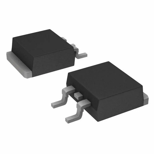
Housed in a TO-263-3 (D²Pak) surface-mount package with two leads and a tab — the supplier device code is PG-TO263-3-2.