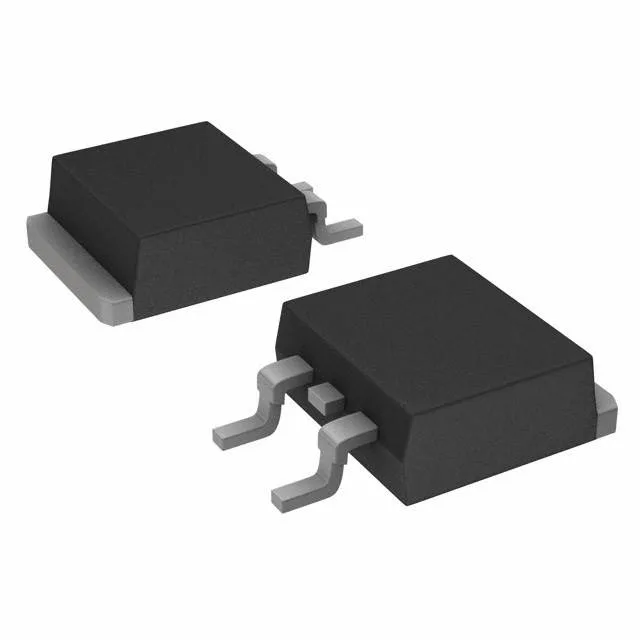
Infineon Technologies IPB073N15N5ATMA1

Infineon IPB073N15N5ATMA1 N-Channel MOSFET, 150V 114A

MPNIPB073N15N5ATMA1
End of Life

Infineon OptiMOS™-5 N-Channel MOSFET, 150 V Vdss, 114 A continuous drain (Tc), 7.3 mOhm Rds(on) at 57 A, 10 Vgs, 61 nC gate charge, TO-263-3 (D²Pak) surface mount, -55°C to 175°C junction.

$5.43Ref. price · indicative, final on quote
PackagingTO-263-3, D²Pak (2 Leads + Tab), TO-263AB
StockContact for availability
MOQ1 pcs
  • 100% new & originalTraceable channels only — no refurbs, no pulls, no remarked parts.
  • Date & lot codes on quoteStated per line before you commit; label photos on request.
  • MSL-compliant ESD packingMoisture-sealed bags with indicator cards; reels photo-verified.
  • PayPal buyer protectionPay by T/T, PayPal or Payoneer — card payments covered end to end.

Specifications

IPB073N15N5ATMA1 Technical Specifications
ParameterValue
SeriesOptiMOS™-5
FET typeN-Channel
Mounting typeSurface Mount
Drain to source voltage150 V
Drive voltage (Max rds on, min rds on)8V, 10V
Current - continuous drain (Id) @ 25°C114A (Tc)
Power dissipation214W (Tc)
Operating temperature-55°C ~ 175°C (TJ)
PackageTape & Reel (TR); Cut Tape (CT)
Vgs±20V
TechnologyMOSFET (Metal Oxide)
CaseTO-263-3, D²Pak (2 Leads + Tab), TO-263AB
Vgs(th) (Max) @ id4.6V @ 160µA
Rds on (Max) @ id, vgs7.3mOhm @ 57A, 10V
Gate charge (Qg) (Max) @ vgs61 nC @ 10 V
Input capacitance (Ciss) (Max) @ vds4700 pF @ 75 V

Product details

150 V Vdss — the voltage class that sets the bus margin

The IPB073N15N5ATMA1 is an Infineon OptiMOS™-5 N-channel power MOSFET with a 150 V drain-to-source breakdown voltage and a continuous drain current rating of 114 A at a case temperature. The 7.3 mOhm on-resistance at 57 A and 10 Vgs gives a conduction-loss floor. The package is rated for 214 W dissipation at the case.

61 nC gate charge and the driver budget

Total gate charge at 10 V is 61 nC. The drive voltage window is 8 V to 10 V for achieving the rated Rds(on). Input capacitance is 4700 pF measured at 75 V Vds.

175 °C junction — thermal headroom for tight enclosures

The maximum junction temperature is 175 °C. In a 214 W dissipation package (Tc) that margin matters when the heatsink is constrained. The threshold voltage is 4.6 V maximum at 160 µA drain current.

TO-263-3 footprint and the exposed tab

The part comes in a TO-263-3 (D²Pak) surface-mount package with the supplier device code PG-TO263-3-2. The exposed drain tab is the primary thermal path — the PCB copper area under the tab sets the junction-to-ambient thermal resistance. This is a standard footprint for 150 A-class MOSFETs in automotive and industrial power stages.

It is ROHS3 compliant.

Frequently asked questions

What is the datasheet for IPB073N15N5ATMA1?

Design engineers need the datasheet to validate electrical characteristics and pin compatibility.

Where can I buy IPB073N15N5ATMA1 with stock in the US?

Sourcing buyers need to quickly identify distributors with available inventory to avoid supply delays.

What is the price of IPB073N15N5ATMA1 in volume?

Commercial buyers compare bulk pricing to optimize BOM cost for production runs.

Is IPB073N15N5ATMA1 a direct replacement for IPB073N15N3?

Maintenance techs and buyers need to know if the newer part can drop-in replace an older or obsolete device without board changes.

What is the lead time for IPB073N15N5ATMA1?

Production planners need lead time estimates to avoid line stoppages and manage procurement schedules.

Is IPB073N15N5ATMA1 obsolete or still active?

Brokers and buyers check lifecycle status to ensure long-term availability and avoid last-time-buy pressures.