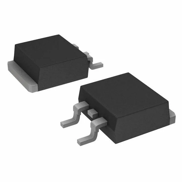
Infineon Technologies IPB057N06NATMA1

IPB057N06NATMA1 Infineon OptiMOS N-Ch 60V 45A D2PAK

MPNIPB057N06NATMA1
End of Life

Infineon OptiMOS series, N-Channel MOSFET, 60 V drain-source, 45 A continuous drain (Tc), 5.7 mOhm max Rds(on) at 10 V, 27 nC gate charge, PG-TO263-3 (D2PAK) surface-mount package, -55°C to 175°C junction temperature.

$1.53Ref. price · indicative, final on quote
PackagingTO-263-3, D²Pak (2 Leads + Tab), TO-263AB
StockContact for availability
MOQ1 pcs
  • 100% new & originalTraceable channels only — no refurbs, no pulls, no remarked parts.
  • Date & lot codes on quoteStated per line before you commit; label photos on request.
  • MSL-compliant ESD packingMoisture-sealed bags with indicator cards; reels photo-verified.
  • PayPal buyer protectionPay by T/T, PayPal or Payoneer — card payments covered end to end.

Specifications

IPB057N06NATMA1 Technical Specifications
ParameterValue
SeriesOptiMOS™
FET typeN-Channel
Mounting typeSurface Mount
Drain to source voltage60 V
Drive voltage (Max rds on, min rds on)6V, 10V
Current - continuous drain (Id) @ 25°C17A (Ta), 45A (Tc)
Power dissipation3W (Ta), 83W (Tc)
Operating temperature-55°C ~ 175°C (TJ)
PackageTape & Reel (TR); Cut Tape (CT)
Vgs±20V
TechnologyMOSFET (Metal Oxide)
CaseTO-263-3, D²Pak (2 Leads + Tab), TO-263AB
Vgs(th) (Max) @ id2.8V @ 36µA
Rds on (Max) @ id, vgs5.7mOhm @ 45A, 10V
Gate charge (Qg) (Max) @ vgs27 nC @ 10 V
Input capacitance (Ciss) (Max) @ vds2000 pF @ 30 V

Product details

Active production, 60 V N-channel for 12 V and 48 V rails

The Infineon IPB057N06NATMA1 is an OptiMOS N-channel power MOSFET rated for 60 V drain-source and 45 A continuous drain current at the case.

175 °C junction — thermal headroom for tight enclosures

The 83 W power dissipation at the case (Tc) assumes a proper thermal interface to a heatsink or PCB copper plane; the 3 W at ambient (Ta) is the free-air limit with no heatsinking.

Gate drive and switching — 27 nC total gate charge

With a 27 nC total gate charge at 10 V, a standard gate driver IC can switch this part at moderate frequencies without excessive drive current. The 2000 pF input capacitance at 30 V drain-source is a typical figure for this on-resistance class; the drive voltage range of 6 V to 10 V lets the designer trade off Rds(on) against gate drive complexity.

D2PAK footprint — thermal and layout considerations

The 2.8 V max gate threshold at 36 µA drain current means a 5 V gate drive from a logic-level source will turn the device on hard, but the 10 V drive is recommended for the lowest Rds(on).

Sourcing and supply posture

ROHS3 compliant. No official second-source or direct replacement is published by Infineon, so dual-sourcing requires qualification of an equivalent N-channel 60 V MOSFET in the same package.

Frequently asked questions

What is the Rds(on) and gate charge for IPB057N06NATMA1?

Maximum on-resistance is 5.7 mOhm at 45 A drain current with 10 V gate drive. Total gate charge is 27 nC at 10 V. These figures set the conduction loss and switching loss budget for the design.

Is IPB057N06NATMA1 RoHS compliant?

Yes, the part is listed as ROHS3 Compliant.