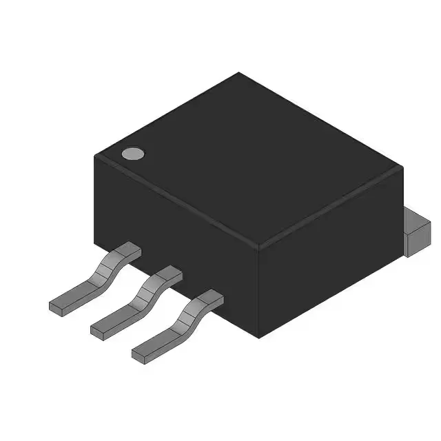
Infineon Technologies IPB051NE8NG

IPB051NE8NG N-Channel MOSFET, 85 V, 5.1 mOhm, TO-263

MPNIPB051NE8NG
End of Life

Infineon OptiMOS™2 IPB051NE8NG, N-Channel MOSFET, 85 V Vdss, 5.1 mOhm Rds(on) @ 100 A, 10 V, 180 nC gate charge, TO-263-3 (D²Pak), -55 to 175 °C.

$1.52Ref. price · indicative, final on quote
PackagingTO-263-3, D²Pak (2 Leads + Tab), TO-263AB
RoHSROHS3 Compliant
SeriesOptiMOS™2
Independent supplier — new & surplus stockAuthenticity-screened · ESD-safe packingListing updated Jul 2026

Specifications

IPB051NE8NG specifications
ParameterValue
SeriesOptiMOS™2
FET typeN-Channel
MountingSurface Mount
Drain to source voltage85 V
Drive voltage (Max rds on, min rds on)10V
Current - continuous drain (Id) @ 25°C100A (Tc)
Power dissipation300W (Tc)
Operating temperature-55°C ~ 175°C (TJ)
PackageBulk
Vgs±20V
TechnologyMOSFET (Metal Oxide)
CaseTO-263-3, D²Pak (2 Leads + Tab), TO-263AB
Vgs(th) (Max) @ id4V @ 250µA
Rds on (Max) @ id, vgs5.1mOhm @ 100A, 10V
Gate charge (Qg) (Max) @ vgs180 nC @ 10 V
Input capacitance (Ciss) (Max) @ vds12100 pF @ 40 V

Product details

Gate charge and switching — what the driver sees

Total gate charge is 180 nC at 10 V, and input capacitance (Ciss) is 12100 pF at 40 V drain — a combination that demands a gate driver capable of sourcing several amperes peak to hit fast switching edges. The maximum gate-source voltage is ±20 V, so a standard 10 V or 12 V gate drive rail is safe; the threshold voltage is 4 V max at 250 µA drain current.

Package and thermal budget

Housed in a TO-263-3 (D²Pak) surface-mount package (PG-TO263-3-2), the part dissipates up to 300 W at the case, but the real thermal limit depends on the PCB copper area under the tab.

Frequently asked questions

What is the gate charge of IPB051NE8NG?

Total gate charge (Qg) is 180 nC at 10 V gate-source voltage.