Total gate charge at 10 V is 117 nC, which sets the driver current requirement: at 100 kHz switching frequency the average gate-drive current is roughly 11.7 mA, well within the capability of a standard half-bridge driver IC. Input capacitance Ciss is 8110 pF at 40 V drain-source — this influences the driver's peak current capability for fast edge rates and the turn-on delay in hard-switched topologies.
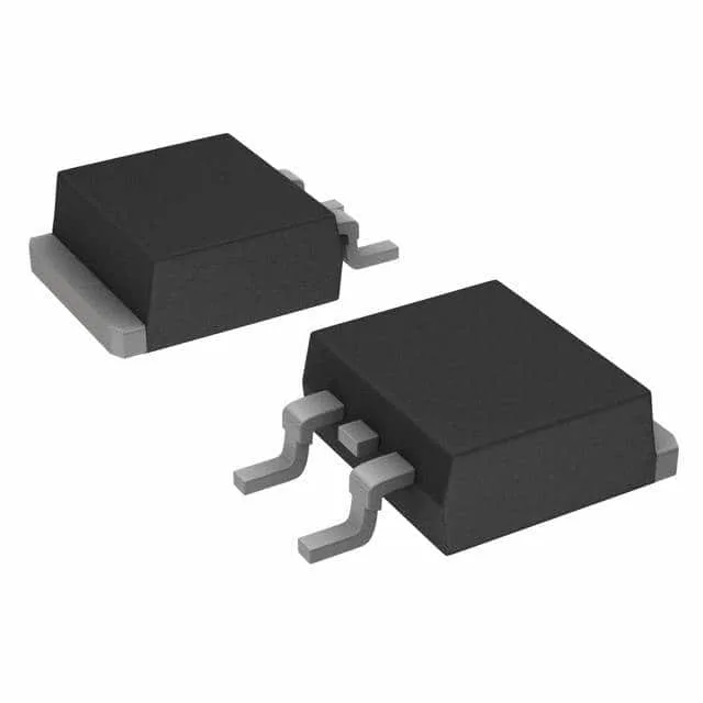
Housed in a TO-263-3 (D²Pak) surface-mount package with the exposed drain tab on the top side. The supplier device code is PG-TO263-3. The gate threshold voltage is 3.5 V maximum at 155 µA drain current, so a 6 V drive is the minimum recommended for full enhancement; 10 V drive achieves the rated Rds(on).
ROHS3 compliant per the lifecycle entry, suitable for lead-free assembly processes.