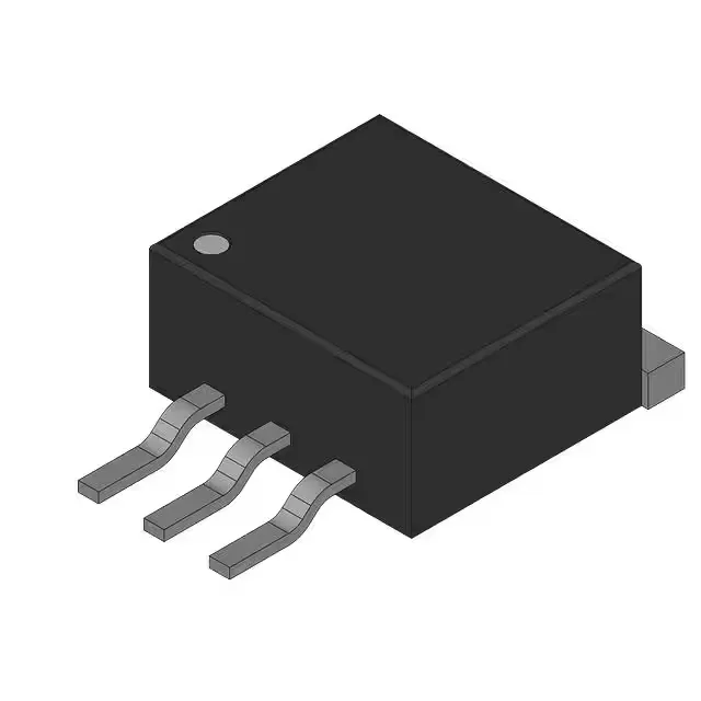
Infineon Technologies IPB022N04LG

Infineon IPB022N04LG N-Channel MOSFET, 40 V, 2.2 mOhm

MPNIPB022N04LG
End of Life

Infineon OptiMOS™ 3, IPB022N04LG, N-Channel MOSFET, 40 V Vdss, 90 A Id, 2.2 mOhm Rds(on) at 10 V, 166 nC Qg, TO-263-3 (D²Pak), -55 to 175 °C.

$0.83Ref. price · indicative, final on quote
PackagingTO-263-3, D²Pak (2 Leads + Tab), TO-263AB
StockContact for availability
MOQ1 pcs
  • 100% new & originalTraceable channels only — no refurbs, no pulls, no remarked parts.
  • Date & lot codes on quoteStated per line before you commit; label photos on request.
  • MSL-compliant ESD packingMoisture-sealed bags with indicator cards; reels photo-verified.
  • PayPal buyer protectionPay by T/T, PayPal or Payoneer — card payments covered end to end.

Specifications

IPB022N04LG Technical Specifications
ParameterValue
SeriesOptiMOS™ 3
FET typeN-Channel
Mounting typeSurface Mount
Drain to source voltage40 V
Drive voltage (Max rds on, min rds on)4.5V, 10V
Current - continuous drain (Id) @ 25°C90A (Tc)
Power dissipation167W (Tc)
Operating temperature-55°C ~ 175°C (TJ)
PackageBulk
Vgs±20V
TechnologyMOSFET (Metal Oxide)
CaseTO-263-3, D²Pak (2 Leads + Tab), TO-263AB
Vgs(th) (Max) @ id2V @ 95µA
Rds on (Max) @ id, vgs2.2mOhm @ 90A, 10V
Gate charge (Qg) (Max) @ vgs166 nC @ 10 V
Input capacitance (Ciss) (Max) @ vds13000 pF @ 20 V

Product details

2.2 mOhm at 90 A — the conduction-loss floor

Its headline spec is a maximum on-resistance of 2.2 mOhm at Vgs = 10 V and Id = 90 A — the lowest Rds(on) in the 40 V OptiMOS 3 portfolio. For a synchronous buck converter or a motor-drive H-bridge, that 2.2 mOhm floor translates directly into conduction loss: at 50 A, the I²R dissipation sits at roughly 5.5 W, well within the 167 W package limit.

175 °C junction — headroom for harsh environments

That extra 25 °C matters in under-hood automotive, industrial motor compartments, or downhole tools where the ambient near the heatsink can push junction spikes past 150 °C.

Gate charge and input capacitance — the driver budget

Total gate charge Qg is 166 nC at Vgs = 10 V, with an input capacitance Ciss of 13000 pF at Vds = 20 V. A 166 nC gate charge at a 100 kHz switching frequency draws 16.6 mA average from the gate driver — a standard 2 A gate-driver IC handles that comfortably, but the 13 nF input capacitance means the driver must source a peak current of several amps during the Miller plateau transition. The PG-TO263-3-2 package (D²Pak) exposes a large copper tab on the bottom for heatsinking; the thermal pad area on the PCB sets the effective RthJA.

Active lifecycle and compliance

It carries ROHS3 compliance, meaning no restricted phthalates or halogenated flame retardants in the package. The series is OptiMOS™ 3, a mature 40 V trench-technology node that has been in volume production for years; the date-code traceability from Infineon's fabs is well-documented, and the laser-etched markings on the TO-263 body are consistent across production lots — a useful check when vetting independent-distributor stock.

Frequently asked questions

Is IPB022N04LG RoHS compliant?

Yes, the IPB022N04LG is rated ROHS3 Compliant, meaning it meets the EU RoHS directive without exemptions for restricted substances including lead, mercury, cadmium, and phthalates.

What is the exact Rds(on) of IPB022N04LG?

The maximum Rds(on) is 2.2 mOhm at Vgs = 10 V and Id = 90 A. This is the worst-case figure across the full operating temperature range; typical values at 25 °C are lower.

What is the maximum drain source voltage of IPB022N04LG?

The drain-to-source breakdown voltage (Vdss) is 40 V. This is the absolute maximum rating; operating continuously at the full 90 A requires derating the voltage below 40 V to stay within the safe operating area.