At elevated junction temperature the on-resistance increases by roughly 50 % at 125 °C — a 120 A load then sees about 2.25 mOhm effective, still low enough to keep I²R conduction loss under 35 W. Gate charge is 250 nC at 10 V, which demands a gate driver capable of sourcing several amperes peak to hit the target switching speed; a 2 A driver with 10 Ω external gate resistor gives a typical turn-on time around 50 ns.
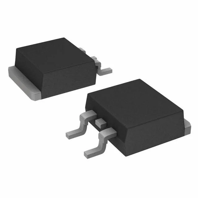
Housed in a PG-TO263-3 (D²Pak) surface-mount package with two leads plus a large tab for heatsinking.
The OptiMOS™ series is Infineon's mainstream low-voltage trench MOSFET portfolio, so supply continuity is stable across package variants.