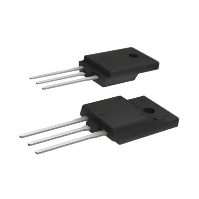
Infineon Technologies IPA037N08N3GXKSA1 — Discrete Semiconductors

Infineon IPA037N08N3GXKSA1 N-Ch 80V 75A MOSFET, TO-220FP

MPNIPA037N08N3GXKSA1
Active

Infineon OptiMOS™ N-channel MOSFET, IPA037N08N3GXKSA1, 80 V, 75 A, 3.7 mOhm Rds(on), TO-220 Full Pack, Through Hole.

$4.7800Ref. price · indicative, final on quote
PackagingTO-220-3 Full Pack
RoHSROHS3 Compliant
SeriesOptiMOS™
Independent supplier — new & surplus stockAuthenticity-screened · ESD-safe packingListing updated Aug 2026

Specifications

IPA037N08N3GXKSA1 specifications
ParameterValue
SeriesOptiMOS™
FET typeN-Channel
MountingThrough Hole
Drain to source voltage80 V
Drive voltage (Max rds on, min rds on)6V, 10V
Current - continuous drain (Id) @ 25°C75A (Tc)
Power dissipation41W (Tc)
Operating temperature-55°C~175°C(TJ)
PackageTube
Vgs±20V
TechnologyMOSFET (Metal Oxide)
CaseTO-220-3 Full Pack
Vgs(th) (Max) @ id3.5V @ 155µA
Rds on (Max) @ id, vgs3.7mOhm @ 75A, 10V
Gate charge (Qg) (Max) @ vgs117 nC @ 10 V
Input capacitance (Ciss) (Max) @ vds8110 pF @ 40 V

Product details

80 V, 75 A N-channel in a fully isolated TO-220

The IPA037N08N3GXKSA1: That saves assembly time and improves thermal contact.

Maximum on-resistance is 3.7 mOhm at 75 A with a 10 V gate drive — that is the figure for sizing conduction losses. At 75 A, I²R loss is about 21 W, which is half the 41 W power dissipation limit of the Full Pack package. In practice, the continuous current at elevated ambient will be lower; the package's thermal resistance to the heatsink sets the real ceiling. Gate charge totals 117 nC at 10 V. A driver with at least 2 A peak source/sink keeps the switching edges clean. The threshold voltage is 3.5 V max at 155 µA drain, and the recommended drive voltage range is 6 V to 10 V. A 5 V logic-level gate signal will not fully enhance this FET — you need a 10 V rail or a gate driver that boosts above the threshold.

Temperature range and compliance

The device is marked as Active in production and fully RoHS3 compliant.