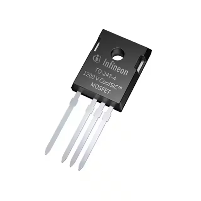
This is a through-hole device in the TO-247-4 package (PG-TO247-4-1), which adds a dedicated Kelvin-source pin to decouple the gate-drive loop from the power path — a feature that reduces switching losses and gate ringing in hard-switched topologies. The 78 mOhm maximum on-resistance at 18 V gate drive and 13 A sets the conduction-loss baseline for efficiency calculations in high-voltage DC-DC, on-board charger, and traction-inverter designs.
Gate drive and switching — 31 nC Qg at 18 V
The device specifies a gate-charge maximum of 31 nC at 18 V, which is moderate for a 1.2 kV SiC FET and keeps driver losses manageable. The recommended drive voltage range for achieving the rated Rds(on) is 15 V to 18 V; the absolute maximum gate-source voltage is +23 V and -7 V. The gate-threshold maximum is 5.7 V at 5.6 mA, so a standard +15 V / -5 V gate drive is well within the safe operating window. Input capacitance is 1060 pF at 800 V Vds, giving a moderate switching speed that simplifies layout parasitics.
Package and thermal — TO-247-4 with Kelvin source
The TO-247-4 package (PG-TO247-4-1) is a through-hole, 4-pin variant. The fourth pin is the Kelvin source connection, which routes the gate return directly to the source pad inside the package, bypassing the current-carrying source bond wires. This reduces the common-source inductance in the gate loop and improves switching performance, particularly at higher frequencies. The maximum power dissipation is 150 W at case temperature, so a heatsink with adequate thermal interface is assumed for continuous operation at the rated current. The device is ROHS3 compliant.