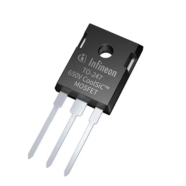
Infineon Technologies IMW65R083M1HXKSA1

Infineon IMW65R083M1HXKSA1 CoolSiC™ N-Channel SiC MOSFET

MPNIMW65R083M1HXKSA1
End of Life

Infineon CoolSiC™ IMW65R083M1HXKSA1, N-channel SiCFET, 650 V Vdss, 111 mOhm Rds(on) at 18 V, 19 nC gate charge, 24 A continuous drain, TO-247-3 through-hole, -55°C to 175°C junction.

$12.65Ref. price · indicative, final on quote
PackagingTO-247-3
StockContact for availability
MOQ1 pcs
  • 100% new & originalTraceable channels only — no refurbs, no pulls, no remarked parts.
  • Date & lot codes on quoteStated per line before you commit; label photos on request.
  • MSL-compliant ESD packingMoisture-sealed bags with indicator cards; reels photo-verified.
  • PayPal buyer protectionPay by T/T, PayPal or Payoneer — card payments covered end to end.

Specifications

IMW65R083M1HXKSA1 Technical Specifications
ParameterValue
SeriesCoolSiC™
FET typeN-Channel
Mounting typeThrough Hole
Drain to source voltage650 V
Drive voltage (Max rds on, min rds on)18V
Current - continuous drain (Id) @ 25°C24A (Tc)
Power dissipation104W (Tc)
Operating temperature-55°C ~ 175°C (TJ)
PackageTube
Vgs+20V, -2V
TechnologySiCFET (Silicon Carbide)
CaseTO-247-3
Vgs(th) (Max) @ id5.7V @ 3.3mA
Rds on (Max) @ id, vgs111mOhm @ 11.2A, 18V
Gate charge (Qg) (Max) @ vgs19 nC @ 18 V
Input capacitance (Ciss) (Max) @ vds624 pF @ 400 V

Product details

650 V SiC MOSFET in a TO-247 — what it brings to the power stage

The IMW65R083M1HXKSA1: It comes in a through-hole TO-247-3 package (PG-TO247-3-41) that handles the 104 W power dissipation without the thermal bottleneck of a surface-mount tab. The maximum Rds(on) is 111 mOhm at 11.2 A drain current with an 18 V gate drive. Gate charge totals 19 nC at 18 V.

At 111 mOhm max, the conduction loss at 11.2 A is within the 104 W package limit. The 19 nC total gate charge at 18 V is sourced by a standard isolated gate driver. Input capacitance Ciss is 624 pF at 400 V drain-source — that is the capacitance the driver charges and discharges each cycle. The low value relative to the 650 V rating is a SiC advantage: the Miller plateau is short, so the switching transition time stays tight even with moderate gate resistance.

Temperature range and mounting — where this part lives

The 175°C junction temperature ceiling provides headroom in a fault condition. Through-hole TO-247-3 with a PG-TO247-3-41 variant — the tab is the drain, and the two source pins are paralleled inside the package to spread the current. The large tab area makes rework straightforward: a hot-air station on the backside while the solder joints melt from the front, no risk of lifting a pad the way a D²PAK can.

Frequently asked questions

What is the Rds(on) and gate charge of IMW65R083M1HXKSA1?

Total gate charge is 19 nC at 18 V.