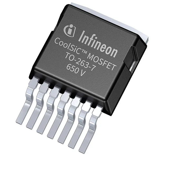
650 V SiC MOSFET for hard-switched power stages
It is built for hard-switched power converters where the wide bandgap material buys lower switching losses than a comparable super-junction Si MOSFET. With a gate charge of only 6 nC at 18 V, the drive energy per switching cycle is low, which keeps the gate-drive power supply small and the switching-node dv/dt manageable.
175°C junction — the thermal envelope
The junction temperature range extends from -55°C to 175°C. That 175°C ceiling is 25°C higher than the typical 150°C limit of a silicon CoolMOS part like the IPD50R950CEAUMA1, which matters when the heatsink is sized for a high ambient or the load cycle pushes the die temperature above 150°C for sustained periods. Maximum power dissipation is 65 W at case temperature Tc.
It is ROHS3 compliant and available through independent distribution. There is no official second-source or direct replacement from Infineon — the CoolSIC M1 is a proprietary SiC process, not a cross-licensed die. For dual-sourcing, evaluate a functionally similar SiC MOSFET from a different foundry, but confirm the gate-drive voltage (18 V nominal) and the pinout of the PG-TO263-7-12 footprint.
Gate-drive and switching note
The recommended drive voltage for minimum on-resistance is 18 V. Maximum gate-source ratings are +23 V and -5 V, so a standard 15 V or 18 V gate-drive supply with a negative turn-off rail (e.g. -3 V to -5 V) stays within the negative limit. The input capacitance Ciss is 201 pF at 400 V drain-source — the gate-drive current needed to charge and discharge that capacitance at the target switching frequency is modest, but the driver must source the peak current to switch the gate charge in the desired transition time.