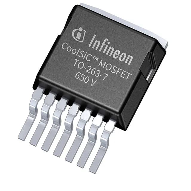
Infineon Technologies IMBG65R048M1HXTMA1

Infineon IMBG65R048M1HXTMA1 CoolSiC™ N-Ch SiCFET, 650 V

MPNIMBG65R048M1HXTMA1
End of Life

Infineon CoolSiC™ series, IMBG65R048M1HXTMA1, N-Channel SiCFET, 650 V Vdss, 45 A Id, 64 mOhm Rds(on) max @ 18 V, 33 nC Qg, PG-TO263-7-12, -55 to 175 °C.

$11.64Ref. price · indicative, final on quote
PackagingPG-TO263-7-12
StockContact for availability
MOQ1 pcs
  • 100% new & originalTraceable channels only — no refurbs, no pulls, no remarked parts.
  • Date & lot codes on quoteStated per line before you commit; label photos on request.
  • MSL-compliant ESD packingMoisture-sealed bags with indicator cards; reels photo-verified.
  • PayPal buyer protectionPay by T/T, PayPal or Payoneer — card payments covered end to end.

Specifications

IMBG65R048M1HXTMA1 Technical Specifications
ParameterValue
SeriesCoolSiC™
FET typeN-Channel
Mounting typeSurface Mount
Drain to source voltage650 V
Drive voltage (Max rds on, min rds on)18V
Current - continuous drain (Id) @ 25°C45A (Tc)
Power dissipation183W (Tc)
Operating temperature-55°C ~ 175°C (TJ)
PackageTape & Reel (TR); Cut Tape (CT)
Vgs+23V, -5V
TechnologySiCFET (Silicon Carbide)
Vgs(th) (Max) @ id5.7V @ 6mA
Rds on (Max) @ id, vgs64mOhm @ 20.1A, 18V
Gate charge (Qg) (Max) @ vgs33 nC @ 18 V
Input capacitance (Ciss) (Max) @ vds1118 pF @ 400 V

Product details

650 V SiC MOSFET — what the 64 mOhm Rds(on) means on your power stage

The Infineon IMBG65R048M1HXTMA1 is a CoolSiC™ N-channel silicon carbide MOSFET in a PG-TO263-7-12 surface-mount package. The 64 mOhm Rds(on) at 18 V gate drive is the number that sets your conduction loss budget. At 20 A load current, I²R loss runs about 26 W — that's the heat the package has to sink through the TO263-7 tab. The 183 W power dissipation rating at the case gives you headroom if you keep the junction below 175°C. Gate charge is 33 nC at 18 V. That's low enough that a standard MOSFET driver with 2 A peak current can switch it at 100 kHz with about 3.3 mA average drive current. The input capacitance is 1118 pF at 400 V drain bias — the low Ciss at high Vds is a SiC advantage that reduces driver-side switching loss at light loads.

Junction temperature ceiling — 175°C vs the usual 150°C

The operating junction temperature range runs from -55°C to 175°C. That 175°C upper limit is 25°C higher than most silicon CoolMOS™ parts can manage. In a compact 650 V power stage — say a 2 kW totem-pole PFC or a 1.5 kW DC-DC converter — that extra thermal margin means you can shrink the heatsink or push more current before hitting the derating curve. The gate threshold voltage maximum is 5.7 V at 6 mA drain current. With a recommended drive voltage of 18 V for minimum Rds(on), the gate overdrive is about 12 V — well clear of the threshold window and safely inside the +23 V / -5 V absolute maximum gate rating.

Active production and compliance — no LTB clock ticking

ROHS3 compliance is confirmed.

Frequently asked questions

What is the Rds(on) of IMBG65R048M1HXTMA1 at 18V gate drive?

The maximum Rds(on) is 64 mOhm at 20.1 A drain current with an 18 V gate drive. That's the worst-case on-resistance across the operating temperature range; typical values at 25°C junction will be lower.

Is IMBG65R048M1HXTMA1 RoHS and REACH compliant?

Yes, the part is ROHS3 compliant per the lifecycle record. REACH compliance is standard for Infineon's current-production CoolSiC™ portfolio, though the specific REACH registration is not listed in this entry.

What is the typical application for the IMBG65R048M1HXTMA1?

This 650 V, 45 A SiC MOSFET is suited for high-efficiency power conversion where switching frequency and thermal margin matter — totem-pole PFC stages, bridgeless boost converters, 1.5–3 kW DC-DC converters, and on-board chargers for electric vehicles. The 175°C junction rating and low Rds(on) make it a fit for compact, forced-air or liquid-cooled power stages.

Can IMBG65R048M1HXTMA1 replace an obsolete SiC MOSFET?

It can replace a 650 V class SiC MOSFET in the same TO263-7 footprint, provided the gate drive is compatible — the recommended drive is 18 V for minimum Rds(on), and the absolute maximum gate voltage is +23 V / -5 V. Check the pinout and gate threshold of the obsolete part against these limits before committing the BOM.