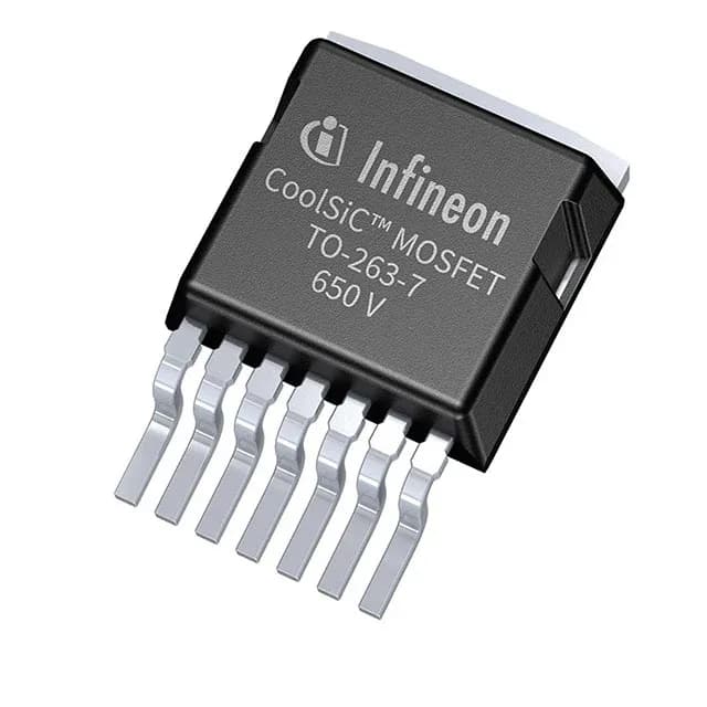
650 V SiC FET for high-density power conversion
The Infineon IMBG65R022M1HXTMA1 is a 650 V N-channel silicon carbide FET from the CoolSiC™ family, built on SiCFET technology for low switching and conduction losses in hard-switched topologies.
Gate drive and switching behavior
This SiC FET requires an 18 V gate drive for the specified 30 mOhm Rds(on) — standard 10 V or 12 V silicon MOSFET drivers will not fully enhance the channel, leaving extra on-resistance on the table. The gate threshold voltage is 5.7 V maximum at 12.3 mA drain current, so a 0 V to 18 V swing with a negative off-state bias (the -5 V Vgs max limit) is the typical drive profile for fast switching. Total gate charge is 67 nC at 18 V, and input capacitance measures 2288 pF at 400 V drain-source bias. These numbers are moderate for a 64 A, 650 V part — expect switching losses to be manageable with a properly sized gate driver in the 2 A to 5 A peak current range.
Package and thermal management
Housed in a PG-TO263-7-12 (D2PAK-7) surface-mount package, this part has a large exposed drain tab for heat sinking through the PCB copper plane. The 300 W power dissipation rating at case temperature assumes adequate thermal management — a multi-layer board with thermal vias under the tab and a heatsink on the opposite side is the typical approach for continuous high-current operation. The 7-lead variant (six source pins plus one gate) distributes the source current and improves thermal conduction compared to the standard 3-lead D2PAK. The footprint is not pin-compatible with a standard TO-263-3 — verify the land pattern before layout.
Lifecycle and supply position
Sourced through independent distribution, this part is quoted to order against your BOM quantity.