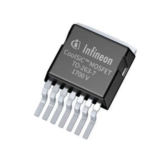
1700 V SiC FET for high-voltage power conversion
The IMBF170R1K0M1XTMA1: The 1700 V blocking voltage places it above standard 650 V and 900 V MOSFETs — this part targets applications where the DC bus exceeds 1000 V, such as three-phase 690 VAC drives, photovoltaic inverters with 1500 V DC input, and high-voltage auxiliary power supplies. The 1000 mOhm maximum on-resistance at 1 A and 15 V gate drive is higher than lower-voltage SiC parts, but the Rds(on) × Qg figure of merit is competitive for the voltage class — 1000 mOhm × 5 nC = 5000 mOhm·nC, enabling efficient switching at moderate frequencies.
Gate drive and switching performance
Gate charge is 5 nC typical at 12 V, and the recommended drive voltage range is 12 V to 15 V for achieving the rated Rds(on). The low Qg means the gate driver only needs to supply about 0.5 mA average current per MHz of switching frequency — a standard 1 A gate driver can easily drive multiple paralleled devices without excessive power dissipation. Input capacitance is 275 pF at 1000 V drain-source bias, which keeps the switching transition times short. The combination of low Ciss and low Qg makes this FET suitable for hard-switching topologies up to several hundred kHz, limited primarily by the thermal management of the 68 W maximum power dissipation. The gate-source voltage range of +20 V to -10 V provides margin for gate-drive overshoot during fast switching — a common concern with SiC devices where the Miller plateau can push the gate voltage above the recommended operating point.
Package and thermal interface
Housed in a PG-TO263-7-13 package (TO-263 with 7 leads and an exposed tab), the part is surface-mountable with the drain tab soldered to the PCB copper plane for heat sinking. The 68 W power dissipation at case temperature requires a thermal design that keeps the junction below 175°C — the exposed tab should connect to a copper area of at least 2-3 square inches on a 2 oz copper PCB for continuous operation at rated current. The wide temperature margin allows for derating in high-ambient installations without exceeding the junction limit.