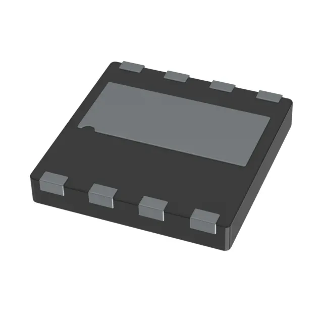
The 157 pF input capacitance at 400 V drain bias is the headline number that separates GaN from silicon. The PG-LSON-8-1 package (8-lead LDFN with exposed pad) is a surface-mount footprint.
Gate drive — the GaN constraint that catches Si designers
Because GaN FETs have no intrinsic body diode, the reverse conduction characteristic is different from a MOSFET. The device conducts in the third quadrant with a Vsd that depends on gate bias. This matters for half-bridge and synchronous-rectifier designs where dead-time conduction loss must be calculated from the GaN's own curve, not a diode forward drop.
That is the full military-temperature-grade span, which in practice means this part is at home in outdoor telecom rectifiers, industrial motor drives with high ambient temperatures, and on-board chargers for electric vehicles where the thermal cycling is severe. The -55 °C low end covers cold-soak startup in arctic environments without parameter drift concerns.
Infineon continues to manufacture the CoolGaN series in this package variant. The part is ROHS3 compliant.