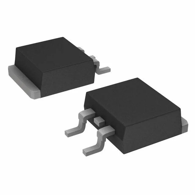
650 V, 80 A TrenchStop 5 — the power-stage workhorse
The Infineon IGB50N65H5ATMA1 is a 650 V, 80 A Trench Field Stop IGBT from the TrenchStop 5 series, in a surface-mount PG-TO263-3 (D²Pak) package. It targets hard-switching applications like motor drives, UPS inverters, and PFC stages where conduction and switching losses must balance. The 650 V collector-emitter breakdown gives a comfortable derating margin on a 400 VDC bus — the standard intermediate rail in three-phase industrial drives and solar inverters.
Conduction and switching — the loss budget
At this operating point the conduction loss is 105 W, which combined with the 270 W package limit means the thermal design — heatsink, airflow, PCB copper — is the real constraint, not the die itself. Total gate charge is 120 nC, a moderate figure that a standard IGBT driver IC (e.g., 2 A peak source/sink) can switch in the 10–20 kHz range without excessive drive power. The test condition of 400 V, 50 A, 12 Ohm gate resistor, 15 V gate drive yields turn-on energy of 1.59 mJ and turn-off energy of 750 µJ — the switching loss per cycle at 16 kHz would be about 37 W, which must be added to the conduction loss for the total thermal budget. Turn-on delay is 23 ns and turn-off delay is 173 ns at 25°C. The 150 ns asymmetry means the dead-time setting in the inverter bridge must accommodate the longer turn-off delay to prevent shoot-through.
Package and thermal — D²Pak layout notes
The PG-TO263-3 (D²Pak) surface-mount package has an exposed metal tab that is electrically connected to the collector. The PCB footprint must include a thermal pad with multiple vias to the inner-layer copper planes to pull heat away from the tab. The 270 W maximum power dissipation is achievable only with adequate heatsinking — a two-layer board with minimal copper will derate that figure significantly. The 80 A continuous collector rating and 150 A pulsed rating mean the PCB traces and solder joints must be sized for the peak current, not just the DC average.
Lifecycle and compliance — active for new designs
For dual-sourcing, the buyer should qualify a second IGBT from a different manufacturer with matching 650 V / 80 A / TO-263 ratings.