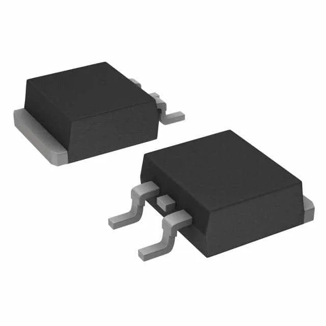
It is a standard-input, single-switch device aimed at medium-frequency hard-switching applications like PFC boost stages, motor-drive inverters up to about 1 kW, and induction-heating resonant converters where the 20 A continuous rating gives headroom for 10–15 A RMS load current with a decent heatsink.
62 nC gate charge — sizing the driver
The 62 nC total gate charge is the number that tells you whether your existing gate-driver IC can turn this IGBT on and off fast enough. At a 20 kHz switching frequency, the average gate-drive current needed is 62 nC × 20 kHz = 1.24 mA — trivial. At 100 kHz, that becomes 6.2 mA, still within a standard totem-pole driver's capability. The real limit is the peak current: the driver must supply that 62 nC in the desired turn-on time. A 2 A gate driver charges the gate in about 30 ns; a 0.5 A driver takes about 120 ns. The 12 ns turn-on delay and 215 ns turn-off delay at 25 °C are the internal propagation delays — the actual switching speed is set by the external gate resistor and driver current.
2.05 V Vce(on) and 430 µJ switching loss — the thermal trade-off
The 2.05 V typical saturation voltage at 15 V gate drive and 10 A collector current defines the conduction loss: at 10 A, that's 20.5 W of dissipation in the IGBT alone. The 430 µJ switching energy (tested at 400 V, 10 A, 23 Ω gate resistor, 15 V gate drive) adds a frequency-dependent loss. At 20 kHz, switching loss adds about 8.6 W, bringing total die dissipation to roughly 29 W. The 110 W maximum power rating gives thermal headroom, but the TO-263 package's junction-to-case thermal resistance will be the practical limiter — expect to need a heatsink with forced air or a large copper area on the PCB tab pad.
The TO-263-3 package is a standard Infineon PG-TO263-3-2 footprint, shared with many other 600 V IGBTs in the same family, which simplifies second-sourcing if needed.
Package and thermal design note
The tab is electrically live at the collector potential, so the PCB copper pad under it must be connected to the collector node and sized for heat spreading. A 4-layer board with thermal vias under the tab dropping to an inner ground plane is the usual approach for dissipating the 20–30 W typical in a hard-switching application.