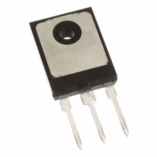
Infineon Technologies IDW40G65C5BXKSA2

Infineon IDW40G65C5BXKSA2 SiC Schottky Diode, 650 V 20 A

MPNIDW40G65C5BXKSA2
End of Life

Infineon CoolSiC™+ IDW40G65C5BXKSA2, Silicon Carbide Schottky Diode, 650 V, 20 A, No Recovery Time > 500 mA (Io), TO-247-3, Through Hole, -55°C to 175°C.

$19.93Ref. price · indicative, final on quote
PackagingTO-247-3
StockContact for availability
MOQ1 pcs
  • 100% new & originalTraceable channels only — no refurbs, no pulls, no remarked parts.
  • Date & lot codes on quoteStated per line before you commit; label photos on request.
  • MSL-compliant ESD packingMoisture-sealed bags with indicator cards; reels photo-verified.
  • PayPal buyer protectionPay by T/T, PayPal or Payoneer — card payments covered end to end.

Specifications

IDW40G65C5BXKSA2 Technical Specifications
ParameterValue
SeriesCoolSiC™+
Diode typeSilicon Carbide Schottky
Mounting typeThrough Hole
Voltage - DC reverse (Vr)650 V
Voltage - forward (Vf) (Max) @ if1.7 V @ 20 A
Current - reverse leakage @ vr210 µA @ 650 V
Current - average rectified20A
Operating temperature - junction-55°C ~ 175°C
SpeedNo Recovery Time > 500mA (Io)
PackageTube
CaseTO-247-3
Capacitance @ vr, f590pF @ 1V, 1MHz
Reverse recovery time0 ns

Product details

650 V / 20 A SiC Schottky — zero-recovery switching

The Infineon IDW40G65C5BXKSA2 is a silicon carbide Schottky diode from the CoolSiC+ series, rated 650 V reverse voltage and 20 A average forward current in a through-hole TO-247-3 package. Its headline spec — zero reverse recovery time (trr = 0 ns) — means there is no stored charge to sweep out during turn-off, so switching losses are effectively eliminated in the diode itself. This is the main reason designers pick SiC over ultrafast silicon in hard-switched PFC, LLC resonant converters, and high-frequency boost stages.

Forward drop and thermal headroom

Maximum forward voltage is 1.7 V at 20 A. Reverse leakage at 650 V is 210 µA.

Package and mounting — TO-247-3

The PG-TO247-3 package uses the standard TO-247 footprint with three through-hole leads. The large copper tab on the back carries the cathode and is the primary thermal path — a pad area on the PCB or a clip-on heatsink with thermal interface material sets the junction-to-case resistance. No exposed paddle to solder; the tab is electrically live (cathode potential), so the heatsink must be isolated or the mounting hole kept clear.

Lifecycle and supply posture

It is RoHS3 compliant (lead-free).

Frequently asked questions

Is IDW40G65C5BXKSA2 compatible with high-frequency power conversion?

Yes — the zero reverse recovery time (trr = 0 ns) eliminates the stored-charge switching loss that limits ultrafast silicon diodes. This makes the part well suited for hard-switched topologies like PFC and LLC converters operating above 100 kHz.