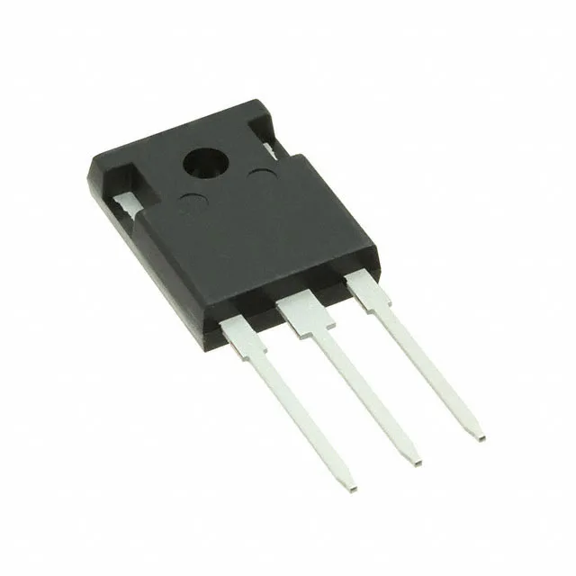
Zero-recovery SiC Schottky — what the 0 ns trr means for the switching stage
The IDW24G65C5BXKSA2 is a 650 V, 12 A silicon-carbide Schottky diode from Infineon's CoolSiC™+ generation, in a PG-TO247-3 through-hole package. Its defining characteristic is a reverse recovery time of 0 ns — a hard-switching benefit that eliminates the recovery charge and tail current of a conventional fast-recovery diode, so the MOSFET or IGBT in the same leg sees no additional turn-on loss from the diode.
Thermal headroom and forward drop at rated current
Reverse leakage at the 650 V blocking voltage is 190 µA — a figure that climbs with junction temperature, so the standby dissipation at high-Tj needs to be budgeted in the thermal model, particularly for light-load or no-load conditions. Capacitance measures 360 pF at 1 V bias, 1 MHz — a low value that reduces the capacitive turn-on energy per cycle in hard-switched topologies like totem-pole PFC or dual-active-bridge converters.
Package, compliance, and sourcing posture
The PG-TO247-3 leadframe is Infineon's own variant; the three through-hole pins fit a standard TO-247 footprint, but the centre-pin tab is the anode, so confirm the pad assignment against the existing board layout before committing the BOM line.