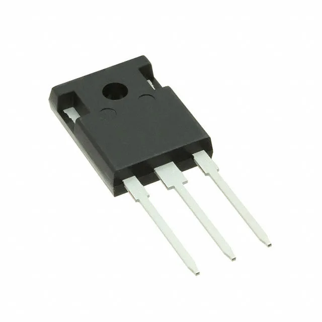
650 V, 10 A SiC Schottky — what the zero trr means on your bench
That makes it a drop-in replacement for slower silicon ultrafast diodes in hard-switching topologies where every nanosecond of recovery adds heat.
Zero recovery — what it saves in the power stage
With trr at 0 ns, there is no reverse-recovery current spike at turn-off. The diode stops conducting the instant the voltage reverses, which eliminates the switching loss term that dominates in silicon ultrafast diodes. In a continuous-conduction-mode PFC or a hard-switched inverter, that translates directly into lower heatsink temperature or higher switching frequency for the same thermal budget. The forward voltage drop is 1.7 V maximum at 10 A — a typical figure for a 650 V SiC Schottky of this die size.
The PG-TO247-3 package is a standard three-lead through-hole with a large backside tab. It takes a soldering iron or a hot-air station with a nozzle that can wet the tab — the thermal mass is substantial, so preheat the board to 100-120 °C before hitting it with the iron. The tab is the drain/cathode; the two outer pins are the anode. The 0.50 mm pitch between leads is generous enough that you can rework it with basic tools, but the tab pad on the PCB needs a thermal relief to avoid cold joints.