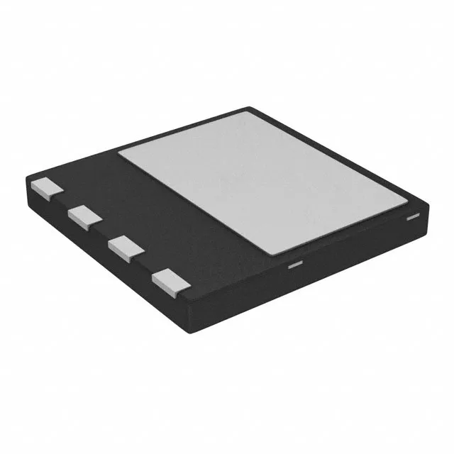
Infineon Technologies IDL10G65C5XUMA2

Infineon IDL10G65C5XUMA2 SiC Schottky Diode, 650V 10A

MPNIDL10G65C5XUMA2
End of Life

Infineon CoolSiC+ IDL10G65C5XUMA2, Silicon Carbide Schottky Diode, 650 V DC reverse voltage, 10 A average rectified current, 0 ns reverse recovery time, surface mount 4-PowerTSFN / PG-VSON-4 package, -55 to 150 °C junction temperature.

$4.56Ref. price · indicative, final on quote
Packaging4-PowerTSFN
RoHSROHS3 Compliant
SeriesCoolSiC™+
Independent supplier — new & surplus stockAuthenticity-screened · ESD-safe packingListing updated Jul 2026

Specifications

IDL10G65C5XUMA2 specifications
ParameterValue
SeriesCoolSiC™+
Diode typeSilicon Carbide Schottky
MountingSurface Mount
Voltage - DC reverse (Vr)650 V
Voltage - forward (Vf) (Max) @ if1.7 V @ 10 A
Current - reverse leakage @ vr180 µA @ 650 V
Current - average rectified10A
Operating temperature - junction-55°C ~ 150°C
SpeedNo Recovery Time > 500mA (Io)
PackageTape & Reel (TR); Cut Tape (CT)
Case4-PowerTSFN
Capacitance @ vr,300pF @ 1V, 1MHz
Reverse recovery time0 ns

Product details

The IDL10G65C5XUMA2 is an Infineon CoolSiC+ silicon carbide Schottky diode rated at 650 V DC reverse voltage and 10 A average rectified current. Its defining characteristic is zero reverse recovery time — the datasheet lists 0 ns trr — which means the diode contributes no switching loss component from stored charge clearing. This is the main reason to pick a SiC Schottky over a silicon ultrafast diode in a hard-switched PFC or DC-DC converter: the recovery loss term drops out of the efficiency calculation entirely. Junction temperature spans -55 to 150 °C, covering industrial motor drives, server PSUs, and automotive on-board charger stages.

Forward drop and leakage — the static trade-off

At the full 10 A rated current the forward voltage is 1.7 V maximum. That is higher than a comparable silicon Schottky at the same current, which is the SiC trade-off: you accept higher conduction loss at high load in exchange for eliminating the switching loss that would dominate at high frequency. Reverse leakage at the full 650 V blocking voltage is 180 µA — a figure that rises with junction temperature, so the thermal design should account for the leakage power at the worst-case hot die temperature.

Surface-mount assembly; the small footprint suits compact power stages where board area is tight. The pad layout and solder stencil aperture should follow the Infineon application note for the VSON-4 to get the rated thermal performance.

ROHS3 compliant. No official second source is listed in the record, but the CoolSiC+ family includes several 650 V / 10 A SiC Schottky diodes in comparable packages from Infineon; the exact PG-VSON-4 footprint should be confirmed against the target layout.

Frequently asked questions

Can IDL10G65C5XUMA2 be used in high-frequency switching applications?

Yes. The zero reverse recovery time eliminates the switching loss component from stored charge, which is the main obstacle to raising frequency in silicon diode stages. This makes the part well suited for hard-switched PFC, LLC resonant converters, and other topologies where low switching loss is critical.

Is IDL10G65C5XUMA2 RoHS compliant?

Yes, it is ROHS3 compliant.

What is the closest pin-compatible alternative to IDL10G65C5XUMA2?

No official cross-reference or second source is listed in the available record. The CoolSiC+ family includes several 650 V SiC Schottky diodes, but pin compatibility depends on the exact PG-VSON-4 footprint. Verify the package drawing against any proposed alternative before committing the PCB layout.

Where can I buy IDL10G65C5XUMA2 and what is the lead time?

Contact our sales team for current pricing and lead time on this part. Availability and pricing are confirmed at quote time.