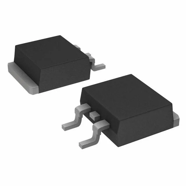
Infineon Technologies IDK12G65C5XTMA2

Infineon IDK12G65C5XTMA2 SiC Schottky Diode, 650 V 12 A

MPNIDK12G65C5XTMA2
End of Life

Infineon CoolSiC™+ IDK12G65C5XTMA2, SiC Schottky diode, 650 V reverse, 12 A average rectified, zero reverse recovery time, TO-263-2 (D²Pak) surface-mount, -55 to 175 °C junction.

$5.39Ref. price · indicative, final on quote
PackagingTO-263-3, D²Pak (2 Leads + Tab), TO-263AB
StockContact for availability
MOQ1 pcs
  • 100% new & originalTraceable channels only — no refurbs, no pulls, no remarked parts.
  • Date & lot codes on quoteStated per line before you commit; label photos on request.
  • MSL-compliant ESD packingMoisture-sealed bags with indicator cards; reels photo-verified.
  • PayPal buyer protectionPay by T/T, PayPal or Payoneer — card payments covered end to end.

Specifications

IDK12G65C5XTMA2 Technical Specifications
ParameterValue
SeriesCoolSiC™+
Mounting typeSurface Mount
Voltage - DC reverse (Vr)650 V
Voltage - forward (Vf) (Max) @ if1.8 V @ 12 A
Current - average rectified12A
Operating temperature - junction-55°C ~ 175°C
SpeedNo Recovery Time > 500mA (Io)
PackageTape & Reel (TR); Cut Tape (CT)
TechnologySiC (Silicon Carbide) Schottky
CaseTO-263-3, D²Pak (2 Leads + Tab), TO-263AB
Capacitance @ vr, f360pF @ 1V, 1MHz
Reverse recovery time0 ns

Product details

Zero reverse recovery — the switching-loss killer

The IDK12G65C5XTMA2 is a 650 V, 12 A SiC Schottky diode from Infineon's CoolSiC™+ series. Its zero reverse recovery time (trr=0 ns) eliminates the switching loss that plagues silicon ultrafast diodes in hard-switched topologies — no recovery charge to sweep out, no tail current, no snubber needed.

650 V / 12 A — where it lands on the power rail

Rated 650 V reverse and 12 A forward average, this diode fits the boost stage of a 400 VDC-bus PFC converter in the 1–2 kW range. The 650 V rating gives 250 V of headroom above the nominal bus — margin for line transients and ring on the switch node. Forward voltage is 1.8 V max at 12 A, 25 °C junction. That sets the conduction loss floor at about 22 W at full rated current — the thermal design must pull that heat out through the TO-263-2 exposed pad. Junction temperature range is -55 °C to 175 °C, the high-temperature ceiling typical of SiC. The 175 °C limit lets the diode run hotter than a 150 °C silicon part, shrinking the heatsink for the same power loss.

Package and thermal path

Supplied in a TO-263-3 (D²Pak) surface-mount package, supplier code PG-TO263-2. The large tab is the cathode and the primary thermal path — PCB copper area under the tab sets the junction-to-ambient thermal resistance. A 2 oz copper pour of at least 600 mm² is typical for this current level. Capacitance is 360 pF at 1 V reverse bias, 1 MHz — relevant for estimating switching losses at light load and for EMI filter design.

Lifecycle and supply posture

Product status is Active per Infineon's current lifecycle record. ROHS3 compliant.

Frequently asked questions

What is the datasheet for IDK12G65C5XTMA2?

Design engineers need complete electrical, thermal, and mechanical specs to validate fit and performance.

Where can I buy IDK12G65C5XTMA2?

Sourcing buyers need immediate links to distributors to check stock and place orders.

What is the price of IDK12G65C5XTMA2?

Price directly impacts BOM cost decisions and procurement budget planning.

Is IDK12G65C5XTMA2 obsolete?

Brokers and maintenance techs need to know lifecycle status to assess risk of supply and plan replacements.

What is the equivalent of IDK12G65C5XTMA2?

When the exact part is unavailable, equivalent parts enable design continuity and avoid redesign.

What is the forward voltage of IDK12G65C5XTMA2 at 12 A?

Forward voltage affects power dissipation and efficiency in circuit design.