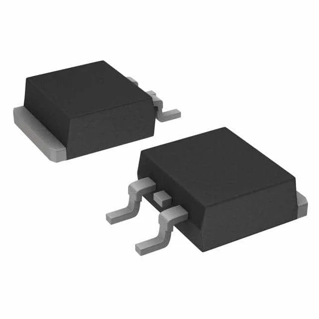
The Infineon IDK08G120C5XTMA1 is a silicon carbide Schottky diode from the CoolSiC™+ family, rated for 1200 V DC reverse and 22.8 A average rectified current. It comes in a PG-TO263-2-1 surface-mount package, which is the D²Pak outline with two leads and a tab for thermal dissipation. The 1200 V blocking voltage puts this part in the high-voltage SiC tier used in power-factor correction (PFC) stages, solar inverters, and EV charging — applications where silicon diodes hit reverse-recovery losses hard. The Schottky structure means zero reverse-recovery charge, so the switching loss is dominated by the junction capacitance, not stored minority carriers.
Forward drop and leakage — the thermal budget drivers
At full rated current the Vf will be higher, so the designer should model the I²R loss at the operating point, not the 8 A test condition. Reverse leakage is 40 µA at 1200 V junction temperature. SiC Schottky leakage rises with temperature but stays orders of magnitude below a comparable silicon ultrafast diode, which matters for standby power in always-on supplies. Junction temperature range extends to 175°C — that is the full SiC capability.
Package and mounting — TO-263-3 layout notes
The PG-TO263-2-1 package is a D²Pak with two leads and a tab — the tab is the cathode. The large copper pad on the PCB should connect to the cathode net with multiple thermal vias to the inner-layer copper plane. The junction-to-case thermal resistance is not listed here, but the tab area is the primary heat path. Capacitance is 365 pF at 1 V and 1 MHz — that is the output capacitance (Coss) that the upstream switch sees during hard switching. It charges and discharges each cycle, adding a frequency-dependent loss term that the designer should include in the switching-loss calculation.