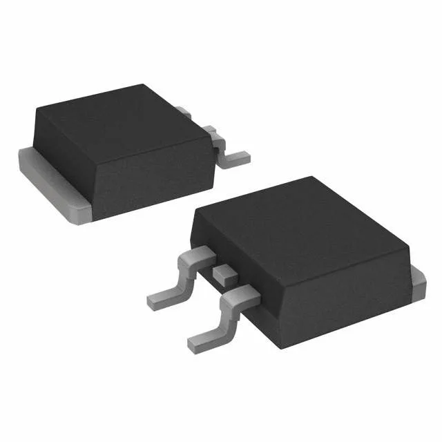
Infineon Technologies IDK06G65C5XTMA2

IDK06G65C5XTMA2 CoolSiC™+ SiC Schottky Diode, 650 V, 6 A

MPNIDK06G65C5XTMA2
End of Life

Infineon CoolSiC™+ IDK06G65C5XTMA2, SiC Schottky diode, 650 V reverse, 6 A average rectified, zero reverse recovery time (trr 0 ns), -55°C to 175°C junction, PG-TO263-2 package.

$2.8Ref. price · indicative, final on quote
PackagingTO-263-3, D²Pak (2 Leads + Tab), TO-263AB
StockContact for availability
MOQ1 pcs
  • 100% new & originalTraceable channels only — no refurbs, no pulls, no remarked parts.
  • Date & lot codes on quoteStated per line before you commit; label photos on request.
  • MSL-compliant ESD packingMoisture-sealed bags with indicator cards; reels photo-verified.
  • PayPal buyer protectionPay by T/T, PayPal or Payoneer — card payments covered end to end.

Specifications

IDK06G65C5XTMA2 Technical Specifications
ParameterValue
SeriesCoolSiC™+
Mounting typeSurface Mount
Voltage - DC reverse (Vr)650 V
Voltage - forward (Vf) (Max) @ if1.8 V @ 6 A
Current - reverse leakage @ vr1.1 mA @ 650 V
Current - average rectified6A
Operating temperature - junction-55°C ~ 175°C
SpeedNo Recovery Time > 500mA (Io)
PackageTape & Reel (TR); Cut Tape (CT)
TechnologySiC (Silicon Carbide) Schottky
CaseTO-263-3, D²Pak (2 Leads + Tab), TO-263AB
Capacitance @ vr, f190pF @ 1V, 1MHz
Reverse recovery time0 ns

Product details

The IDK06G65C5XTMA2 is a 650 V, 6 A SiC Schottky diode from Infineon's CoolSiC™+ family. Its zero reverse recovery time (trr = 0 ns) eliminates the diode reverse-recovery charge that drives turn-on loss in hard-switched topologies — PFC boost stages, LLC converters, and inverter freewheel paths see the biggest efficiency gain.

650 V, 6 A — room to breathe in the power stage

Rated for 650 V DC reverse and 6 A average forward current, this diode fits 400 V bus PFC stages and 350–400 V DC-link applications with healthy derating margin. The forward voltage drop is 1.8 V max at 6 A and 25 °C junction — the conduction loss is set by that Vf × Io product, and it rises with temperature per the SiC curve. Reverse leakage at rated voltage is 1.1 mA at 650 V — typical for a 6 A SiC Schottky, but worth checking against the thermal budget in high-ambient enclosures where leakage doubles with every 10 °C rise.

175 °C junction — high-temp environments covered

That 175 °C ceiling suits designs where the diode sits near hot magnetics or in a sealed PSU enclosure — onboard chargers, server power supplies, industrial motor drives. The part is ROHS3 compliant and can be designed into new production without obsolescence risk.

TO-263-3 package — rework and thermal note

Housed in a PG-TO263-2 (D²Pak, TO-263-3) surface-mount package with an exposed metal tab. The tab is the cathode and the primary thermal path — the board copper area under it sets the junction-to-ambient thermal resistance. Rework with a hot-air station at 300–340 °C, preheat the board to 150 °C to avoid lifting the pad on a thick-copper power plane. Input capacitance is 190 pF at 1 V reverse bias and 1 MHz — low enough that the gate-driver sees negligible capacitive load on the switching node.

Frequently asked questions

What is the IDK06G65C5XTMA2 used for?

It is a 650 V, 6 A SiC Schottky diode used as a boost diode in PFC stages, freewheeling diode in LLC converters, and output rectifier in high-frequency switched-mode power supplies where zero reverse recovery eliminates switching losses.

What is the reverse recovery time of IDK06G65C5XTMA2?

Reverse recovery time is 0 ns — the SiC Schottky barrier has no stored charge, so there is no reverse recovery event. This eliminates the turn-on loss spike in hard-switched converters.

What package does IDK06G65C5XTMA2 come in?

It is supplied in a PG-TO263-2 package, which is a TO-263-3 (D²Pak) surface-mount package with two leads plus the exposed tab. The tab is the cathode connection.